Here you will find out latest app notes.
Behavioral Modeling is the process of developing a model for a device or a system component representing the behavior rather than from a microscopic description. You can use Behavioral Modeling in the domain of analog simulation to model new device types and for black-box modeling of complex systems.
In this document, examples are used to show how the Analog Behavioral Modeling feature of PSpice can be used to:
Assume that you need to create a signal whose voltage is the square root of another signal's voltage. A simple solution is to use a feedback circuit to calculate square roots. But this technique fails if the reference signal goes negative. The solution then is to use the functional form of Analog Behavioral Modeling:
Esqrt out_hi out_lo value={sqrt(abs(v(input)))}
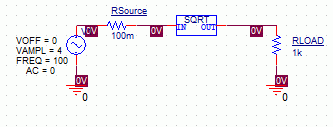
Figure 1: Square Roots Sub-circuit
This model takes the absolute value of the ground-referenced signal input before evaluating the square-root function. The absolute-value function is a nonlinear function.
Note: You can also use a floating signal-pair in the model; for example, replace v(input) with v(in_hi)-v(in_lo) or v(in_hi,in_lo).
You can introduce ideal non-linearity using the table look-up form of Analog Behavioral Modeling. For example, the following one-line, ideal OpAmp model has high gain, but its output is clamped between ±15 volts.:
Eamp out 0 table {200K*(v(in_hi)-v(in_lo))}=
+ (-15,-15) (15,15)
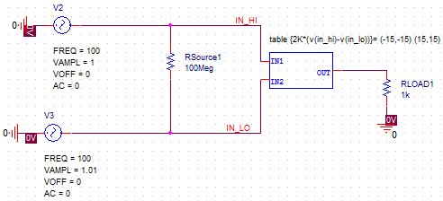
Figure 2: Look-up Tables Sub-circuit
The input to the table is the differential gain formula, but the look-up table has only two entries. The output of the table is interpolated between these two endpoints and clamped when the input exceeds the table's range. This is a convenient use of the table look-up form, available in PSpice.
Square the signalSmall systems of behavioral models are easy to design using PSpice. For example, a true-RMS circuit can be built by decomposing the RMS function:
These three operations can be bundled in a tiny sub-circuit for use as a module:
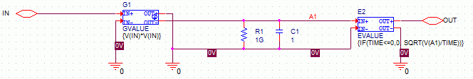
Figure 3: RMS Sub-circuit
.subckt RMS in out G1 0 1 VALUE {V(IN)*V(IN)}
C1 1 0 1 R1 1 0 1G E1 out 0 VALUE {IF(TIME<=0,
0, SQRT(V(1)/TIME))} .ends
The current source, G1, squares the signal, which is then integrated in the capacitor, C1. The voltage on the capacitor is time averaged, and the square-root is taken. The resistor is a dummy load that satisfies the algorithm. The voltage source E1 shows that the value of simulated time is available in Analog Behavioral Modeling, and may be used as a variable in a formula. Note the if-than-else function; If time is less than or equal to zero then the output of E1 is sqrt(v(1)/time). This prevents convergence problems when sqrt(v(1)/time) is evaluated at time = 0.
Parameter passing into sub-circuits also works with Analog Behavioral Modeling, making your models more flexible. Here is a small system that is a voltage follower with hysteresis, useful in simulating, say, a mechanical system with gear backlash:
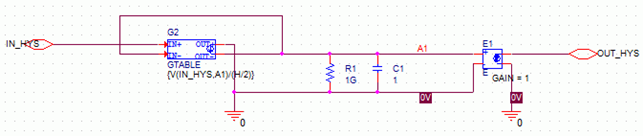
Figure 4: Hysteresis Sub-Circuit
.subckt HYS in out params: H=1 G1 0 1 TABLE
{V(IN,1)/(H/2)} (-2,-1G) (-1,0) (1,0) (2,1G) C1 1 0 1
R1 1 0 1G E1 out 0 1 0 1 .ends
In the model, the parameter H defines the size of the hysteresis, and is used in the formula input to the table. The combination of the formula and table defines a dead-band outside of which the output follows the input with an offset of H/2. The capacitor serves as memory for the circuit and is nearly ideal except for the DC-bias resistor, which provides a droop time constant of one billion seconds. The voltage follower, E1, prevents output loading problems. E1 could also have gain representing the gear ratio of a mechanical system; then voltage would represent the total turn angle of each gear, and H the amount of angular backlash.
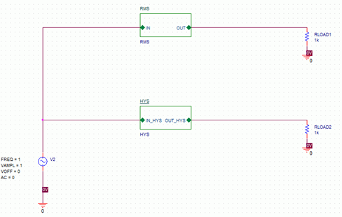
Figure 5: Circuit using RMS and Hysteresis Sub-circuit
.param H=1 * V1 in 0 SIN (0 1 1) Xrms 1 rms RMSXhys 1 hys HYS param: H=1 * .tran 10m 1 .end
A 1Hz sine wave is used for the stimulus to the RMS and HYS circuits.
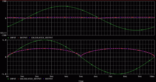
Figure 6: Output from RMS and HYS Circuit
Figure 6 shows a Probe plot of the input, and the outputs from each circuit. Note that the RMS circuit outputs the well-known result of 0.707 volts after one input cycle, while the HYS circuit lags the input by a half volt in each direction for a total hysteresis of one volt.
Multiplier is a behavioral block that performs the mathematical task of multiplying the two inputs, and returns the product as the output. Multipliers are often used for signal processing applications. In this note, two examples are presented to illustrate the use of a multiplier to make an amplitude modulator, and to make a frequency doubler.
Amplitude modulation is a technique which uses a low frequency signal to control the amplitude of a high-frequency signal. A simple modulator can be constructed using a multiplier as shown in Figure 7:
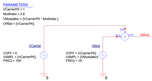
Figure 7: A simple amplitude modulator circuit
One input is the high-frequency or carrier signal, and the other input is the modulating signal.
A sinusoidal source at a frequency of 10 kHz is used to represent the carrier signal and a second source at a frequency of 1 kHz is used to represent the modulating signal. Notice that the peak amplitude for the carrier is set to 1 volt using the parameter VcarrierPK. The modulating index is the ratio of the peak of the modulating signal to the peak of the carrier. Here, the index is set to 0.8 or 80% modulation. A typical broadcast AM signal includes the carrier as well as the sidebands in the transmission. To get such a double sideband transmitted carrier signal (DSBTC) we must bias or offset the modulating signal by a value equal to the carrier's peak voltage.
The amplitude modulated signal and the modulating signal from this simulation are shown in Figure 8
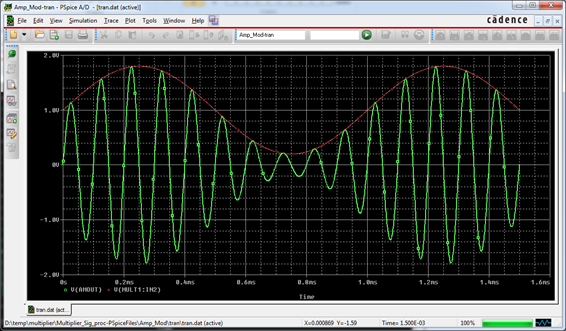
Figure 8: An amplitude modulator output signal
A balanced modulator produces a double sideband suppressed carrier signal (DSB-SC). By setting the offset of the modulating signal to be zero in the above circuit, we will suppress the carrier. Notice, the output of this modulator shown in Figure 9; the shape of its upper A balanced modulator output signal envelope resembles a full-wave rectified AC source.
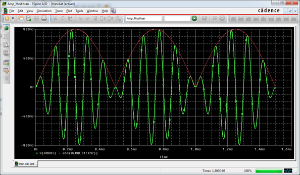
Figure 9: A balanced modulator output siganl
Another application for a multiplier is as a frequency doubler (see Figure 10). Connecting a sinusoidal source simultaneously to both inputs of a multiplier will yield a signal with double the input frequency. The first multiplier, produces a waveform that has one-half the amplitude of the original input signal with a DC offset of one-half the input waveform's peak value. The DC offset is removed with a voltage source called Voffset. The amplitude of the original signal is restored with a second multiplier which doubles the signal.
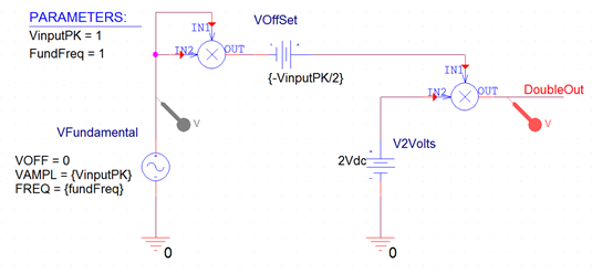
Figure 10: A simple frequency doubler circuit
Figure 11 shows the original input signal, as well as the frequency doubled output signal. These examples have illustrated how a multiplier implemented using the E device in PSpice can be used in signal processing applications such as amplitude modulation and frequency doubling.
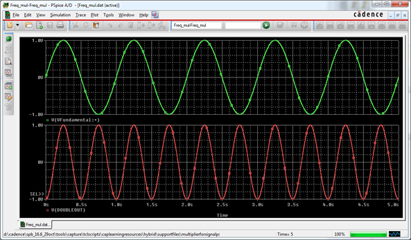
Figure 11: Output results for frequency doubler
Consider a familiar example: the voltage across a parallel capacitor/resistor combination as a function of time. The circuit equation for this example is:PSpice is well known for its ability to solve the equations which arise in circuit analysis. What is less well known is that PSpice can also be used to solve problems in other domains which can be expressed as differential equations. This article presents some examples of using PSpice as an "analog computer" to solve sets of differential equations describing the kinetics of a chemical reaction.
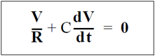
rearranging a little,
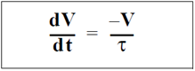
where:
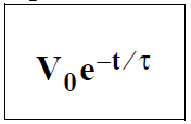
where V0 is the initial voltage on the capacitor.
To see how PSpice can be used to solve the equation above, consider an ideal integrator. Suppose its output is the voltage we want: V. Now the input to the ideal integrator is evidently dV/dt.
A circuit which represents the equation is shown in the following schematic. The schematic was drawn using OrCAD® Capture. The parts shown come from the Analog Behavioral Modeling (ABM) symbol library, "abm.olb," supplied with the program. The symbols INTEG (integrator) and MULT (multiplier) are used.
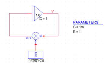
Figure 12: RC circuit
The symbol containing "1.0" is an integrator with gain 1. Its output is obtained by integrating the voltage at its input. This voltage is constrained to be -1/RC times the output voltage, V, by closing the feedback loop.
This way of setting up differential equations for solution is the way that analog computers were used. In this example, an integrator block would be used; the constant 1/RC would be supplied by a gain block and using the inverting input to the integrator would provide the -1.
The initial condition for this problem is that the initial voltage is V0. On an analog computer this voltage would be derived from a reference and patched to the initial condition input of the integrator. Using the ABM integrator symbol, INTEG, the initial voltage is specified by setting the value of the "IC=" attribute on the symbol.
Running a Transient Analysis on the ABM representation of the problem shows the expected exponential decay of voltage with time.
Systems of interest usually contain more than one variable. There may be several interacting voltages in a circuit. In a chemical reaction, the rate of production of a component may depend on the concentrations of several other components.
For example, if we have three components x1, x2, and x3, the equations controlling their rates of decay and production might be:
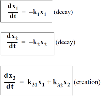
Sets of equations like this can be solved using similar techniques to the first problem. In this example, we would use three integrators with three feedback loops and three node voltages to solve for x1, x2, and x3.
Let's look at a real example. This is a chemical system which contains four components, x1, x2, x3, and x4. They are related by four equations containing "rate constants" (the Ks) and "physical constants" (R and Q):
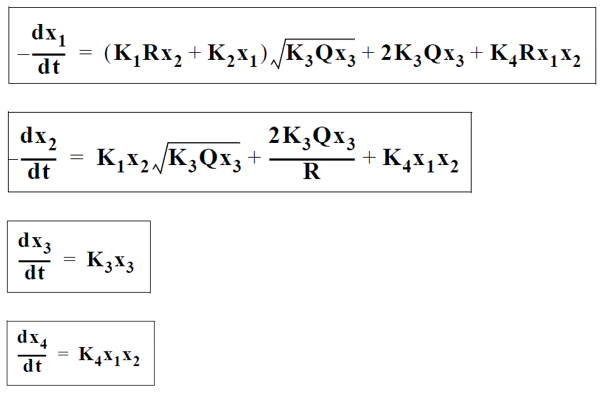
A schematic containing ABM components for integration, summing, and taking square roots, etc., is shown in Figure 13. It also contains definitions for Q and R (the physical constants), and the Ks.
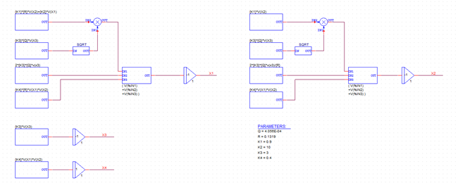
Figure 13: Couples Ordinary Differential Equations(ODE) implemented using ABM components for integration, summing, square roots, etc. the physical constants Q and R are shown, as well as the rate constant, K, to demonstrate a chemical system.
© Copyright 2016 Cadence Design Systems, Inc. All rights reserved. Cadence, the Cadence logo, and Spectre are registered trademarks of Cadence Design Systems, Inc. All others are properties of their respective holders.
Copyright © 2020 Cadence Design Systems, Inc. All rights reserved.