Here you will find out latest app notes.
This document explains the digital worst-case timing simulation feature, to evaluate the timing behavior of Digital and Mixed Analog/Digital designs, as a function of component propagation delay tolerances.
Digital Worst-Case Timing
Digital worst-case timing capability simulates all devices in the Design with the full range of MIN through MAX delays in true "worst-case" mode. Component propagation delays are usually expressed in the .model parameters associated with component types, with -MN, -TY, and -MX suffixes (e.g., TPLHMN ) representing MINimum, TYPical and MAXimum delay values.
These values are obtained from the manufacturer's specification sheets for the components used in the design. In cases where some of these parameters are unspecified, PSpice can establish the missing values by extrapolation. Provided below is an example of MIN and MAX propagation delay specifications for a BUF primitive.
.model T_BUF UGATE ( ; BUF timing model
+ TPLHMN=5ns TPLHTY=8ns TPLHMX=10ns
+ TPHLMN=9ns TPHLTY=10ns TPHLMX=15ns
+ )
PSpice has simplified the use of different timing models, using the property of MNTYMXDLY, for most families of logic. This property can be set on Parts or on the Design.
The values for MNTYMXDLY are:
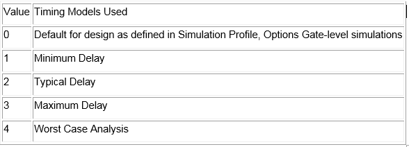
The default value of MNTYMXDLY=0 for each part, while the Timing Mode under Options>> Gate Level Simulation is Worst-Case. Digital worst-case timing simulation can suggest if the digital design would operate as expected, under the worst possible combination of component delay tolerances.
In this regard, worst-case is superior to separate MIN and MAX simulations, which rely on observing circuit behavior only at the extremes of specified tolerances
Figure 1 below shows the Circuit Diagram with Logic Gates having MNTYMXDLY=1
Note: In the attached circuit, make MIN_DELAY as root and select MIN_DELAY-tran as the simulation profile
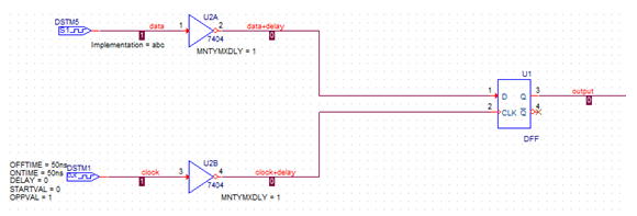
Figure 1: Circuit Diagram with Min Delay Figure 1 Min Delay
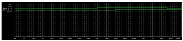
Figure 2: Simulation results with Min Delay
Correct behavior is indeed observed at both extremes of the propagation delay range. Circuit Diagram shown in Figure 3 below has one of the components operating slow with maximum delay and the other component operating fast with minimum delay.
Note: In the attached circuit, make MAX_DELAY as root and then select MAX_DELAY-MAX_DELAY as simulation profile
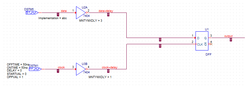
Figure 3: Circuit Diagram with Min and Max delay
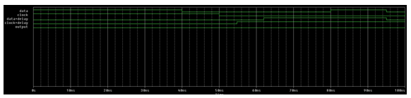
Figure 4: Simulation results with Min and Max Delay
Digital worst-case timing simulation is useful when timing of the signals are critical to the proper operation of Design. In a simple timing simulation (using one of MIN, TYP, or MAX delays), signal propagation through digital devices is normally represented as "instantaneous" transitions, such as those in the examples above.
During worst-case timing simulation, the effects of individual component delay ranges are propagated throughout the circuit. The "transitions" take both the MIN as well as the MAX delay characteristics of their propagation paths; therefore, transitions may be thought of as "regions of signal ambiguity." This is due to the uncertainty of which delay value (MIN, MAX, or somewhere in between) actually applies to each component used in the design. PSpice represents this type of signal ambiguity with "Rising" (R), and "Falling" (F) logic levels.
Circuit Diagram shown in Figure 5 below has both the components operating with worst-case delay.
Note: In attached circuit, make WORSTCASE_DELAY as root and then select WORSTCASE_DELAY-WC_DELAY as simulation profile
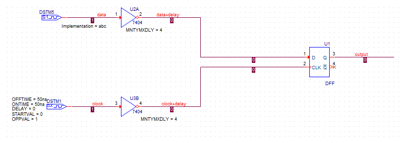
Figure 5: Circuit Diagram with Worst-Case Delay
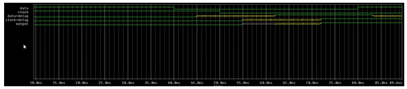
Figure 6: Simulation results with Worst-Case Delay
Note that, due to the uncertainty of the arrival time of both the data and the clock signals, a warning is generated by PSpice, and the output is marked as X' (unknown) from 54.8ns to 62ns.
Other tools called "timing verifiers" are sometimes used in the design process to identify problems that are indigenous to circuit definition. They yield analyses that are inherently pattern- independent, and very often pessimistic, in the sense that they tend to find more problems than will truly exist. This is due to the fact that they do not consider the actual usage of the circuit under applied stimuli.
PSpice does not provide this type of "static" timing verification. Digital worst-case timing simulation, as provided by PSpice, is a pattern-dependent mechanism that allows a designer to locate timing problems subject to the constraints of specific applied stimuli.
Copyright © 2020 Cadence Design Systems, Inc. All rights reserved.