Here you will find out latest app notes.
This document explains Measuring S parameters in PSpice using Probe measurements. It explains obtaining S parameter for a passive circuit (a band pass filter) and an active circuit (transistor circuit).
S-parameters measure the ratio of the incident and reflected signal. The incident signals are defined as a1 and a2. The reflected signals are defined as b1 and b2. The incident and reflected signals are related to voltages and currents at ports 1 and 2 by
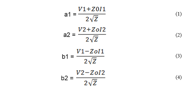
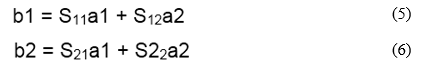
The scattered waves are related to the incident waves by the following set of linear equations:
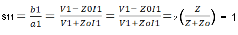
The Sij coefficients are dimensionless ratios; for most applications, the characteristic impedance of the system, Z0, is 50 ohms. S11 is the input reflection ratio and is defined as the ratio of the input port reflected wave to the input incident wave. If the incident wave at the output, a2, is set to zero, then the equations reduce to b1 = S11a1 and b2 = S21a1. Using the defining equations, this reduces to
 (8)
(8)
Where
V1/I1 is the input impedance Z.
S21 is the forward transmission ratio and is defined as the ratio b2/a1.
If the input and output load impedances of the circuit are the same, then S21 is the voltage measured at the output multiplied by 2. If the incident wave at the input is set to zero, then the equations reduce to
b1 = S12a2
b2 = S22a2
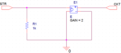
Figure 1: XMITS circuit
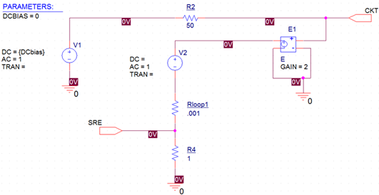
Figure 2: REFLECTS circuit
Create above circuits in Capture and create a hierarchical part for each. For the purpose of this article, these custom parts are named XMITS(Figure. 3) and REFLECTS(Figure. 4), respectively.
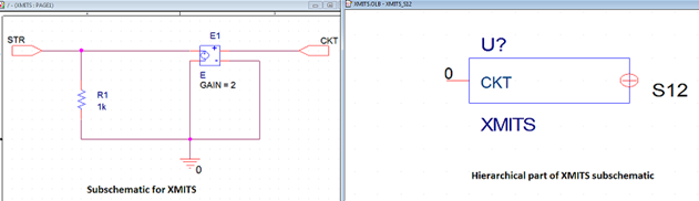
Figure 3: XMITS circuit and its hierarchical part
The XMITS circuit shown in Figure 3 is used to measure the
->Forward transmission coefficient, S21
->Reverse transmission coefficients, S12
Since the output load matches the input load, the transmission coefficients are the output voltage multiplied by 2. The E device, E1, has a gain of 2. The port labeled CKT is used to connect to the external circuit. The port, STR is a hidden pin as shown in Figure. 3. If it is left unconnected in a schematic, OrCAD Capture will generate a unique net. Alternatively, a specific net can be named for the connection by editing the PSpiceDefaultNet attribute value (see Figure. 4) for the XMITS part instance; this way, the STR pin will have a known label ( S21 in this case) when analyzing simulation results within the Probe window.
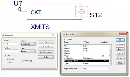
Figure 4: Pin Properties for the XMITS part showing hidden STR pin
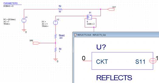
Figure 5: REFLECTS circuit and its hierarchical part
The REFLECTS circuit shown in Figure 2 is used to measure the
->Input reflection coefficient, S11
->Output reflection coefficient, S22
The reflection coefficients are the input voltage multiplied by 2 minus AC unity. The E device, E1, has a gain of 2. As in the transmission coefficients measurement circuit, the interface pin labeled CKT is used to connect to the external circuit. The pin, SRE, is a hidden pin like STR described above, (see Figure. 6). The REFLECTS symbol also has a DCbias property. On active circuits, the DC level can be set on voltage source, V1, by changing the DCbias property for the REFLECTS part instance in OrCAD Capture. By default, this property is set to zero.
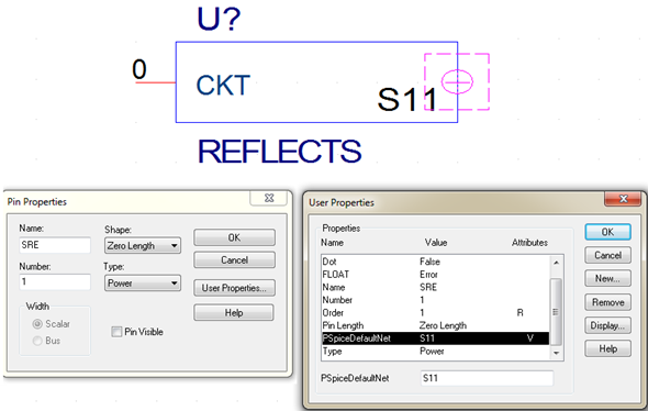
Figure 6: Pin Properties for the Reflects symbol showing hidden S_RE pin
The sub schematics can be used for both passive and active circuits. One can also create and use symbols from these sub schematic in design. Design example referred in this application note uses XMITS and REFLECTS symbols created from these sub schematics. See Creating and Editing Parts in the OrCAD Capture User's Guide for reference to creating hierarchical parts.
The circuit shown in Figure. 7 is a fourth-order Butterworth bandpass filter with a center frequency of 250 MHZ. The first circuit measures S11 and S21. The second circuit measures S12 and S22. For simulation, the AC analysis settings are 500 linear points from 200 MHz to 350 MHZ. The results of the analysis are shown in Figure 8. Extract the attached Test_Case.zip to find the passive folder with this example.
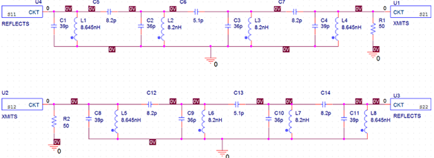
Figure 7: Bandpass filter example
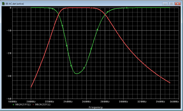
Figure 8: S11 and S21 for the Filter Example
It is also possible to measure the s-parameters of an active circuit. To illustrate this, we have chosen to measure the s-parameters of the RF transistor, MRF5711/MC. Figure 9 shows the circuits for this example.
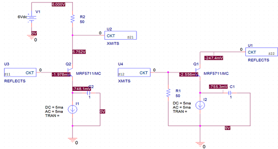
Figure 9: Transistor example
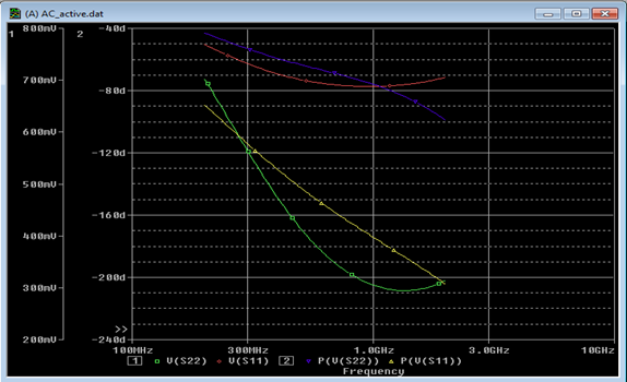
Figure 10: S11 and S22 magnitude and phase
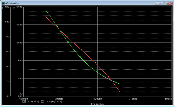
Figure 11: S21 Magnitude and Phase
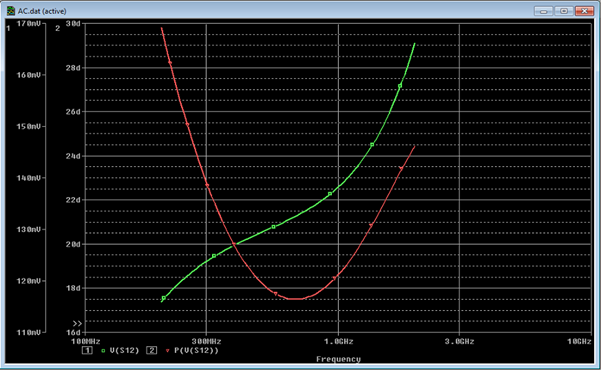
Figure 12: S12 Magnitude and Phase
© Copyright 2016 Cadence Design Systems, Inc. All rights reserved. Cadence, the Cadence logo, and Spectre are registered trademarks of Cadence Design Systems, Inc. All others are properties of their respective holders.
Copyright © 2020 Cadence Design Systems, Inc. All rights reserved.