Here you will find out latest app notes.
The design of electrical systems for military and space applications requires a consideration of the effects of transient and total dose radiation on system performance. Simulation of radiation effects using PSpice helps to identify critical circuit components which could cause system failure and gives guidance for radiation hardening of the system. The information in this application note provides a starting point for those interested in using PSpice for radiation effects analyses.
The design of electrical systems for military and space applications requires a consideration of the effects of transient and total dose radiation on system performance. Simulation of radiation effects using PSpice helps to identify critical circuit components which could cause system failure and gives guidance for radiation hardening of the system. The information in this application note provides a starting point for those interested in using PSpice for radiation effects analyses.
When semiconductor devices such as diodes, transistors, and integrated circuits are exposed to ionizing radiation, such as gamma-rays or X-rays, hole-electron pairs are generated within the semiconductor material. These free carriers result in the generation of photocurrents as they are swept through the depletion regions of the p-n junctions of the device or integrated circuit. The magnitude of these currents can be orders of magnitude greater than normal signal levels and can result in temporary or permanent system failure. PSpice can be easily used to model this type of transient effect.
The magnitudes of the photocurrents are often obtained from experimental data, but can be obtained from theoretical expressions if information on the fabrication process is available. Usually, if an integrated circuit process has been developed for use in a radiation environment, dosimetry measurements have been made on each of the junction types (for example, source, drain and well-to-substrate diffusions in a CMOS technology). Therefore, the photocurrent data is directly available. If no experimental data is available, it is possible for the integrated circuit designer to use a theoretical expression for photocurrent generation. The following equation represents a rectangular pulse of ionizing radiation:

where:
Ipp is the photocurrent in amperes,
gamma is the dose rate in rads(Si)/sec,
q is the electron charge (1.6E-19 coulombs),
g is a constant whose value is 4.2E13 carriers/(rad·cm3),
A is the junction area in cm2,
W is the depletion width in cm,
L is the diffusion length in cm,
tau is the minority carrier lifetime in sec,
tp is the radiation pulse width in sec,
t is time in sec, and
U(t) is a unit step function of time.
For the circuit designer using discrete components, no information is usually available on the process used to fabricate the devices. Dosimetry measurements have been made, however, on a large number of commercial discrete components. This information is often available within aerospace, military and government organizations.
When setting up the circuit description for this type of analysis, photocurrent generators should be placed across all p-n junctions in the design. This must include all parasitic junctions as well as the junctions that make up the explicit design components. Examples of photocurrent generator placement are shown in Figure 1.
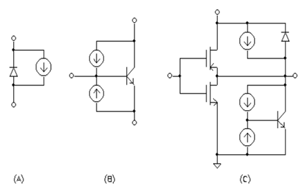
Figure 1: Photocurrent generator placement
Figure 1A and Figure 1B show the proper placement for a diode and a bipolar transistor respectively. These devices could represent discrete components or devices on a bipolar integrated circuit. Figure 1C is an example of the parasitic bipolar diodes and transistors that exist in a CMOS technology. Note that the polarity is such that current flow is from the n-type material to the p-type material.
It is easiest to use a current-controlled current source for photocurrent modeling. For example, assume that you have a small circuit containing only two discrete diodes, both of type DMOD. Further assume that the rest of the circuit consists only of passive components. A portion of the PSpice circuit description is given below.
VPDMOD 1 0 EXP (0 40MV 100NS 8NS 150NS 50NS)
RPDMOD 1 0 1
D12 10 2 DMOD
FD12 10 2 VPDMOD
D20 7 6 DMOD
FD20 7 6 VPDMOD
For an integrated circuit design, the photocurrent modeling process is actually somewhat simpler. Since there are relatively few p-n junction types in a typical integrated circuit technology, the number of controlling sources required will be very small. In this case, define the magnitudes of the controlling sources as current densities. By doing this, the <gain> parameter in the definition of the current-controlled current source becomes the area of the specific p-n junction being modeled.
The following example demonstrates how PSpice can be used to determine the dose rate sensitivity of an integrated circuit. Assume that a die contains a number of diodes all fabricated with the same diffusion and differing only in diode device area. Also assume that dosimetry measurements on this diffusion type have shown a peak current density of 4E-2 amps/cm2 at a dose rate of 1E7 rad(Si)/sec. A small section of a typical circuit description is shown in the following text.
*Radiation effect using ionizing radiation.
.PARAM DOSE_RATE = 1E7 ;initialization
.PARAM JP_MEAS = 4E-2 ;peak measured current density
.PARAM DOSE_MEAS = 1E7 ;at measured dose rate
* perform simulations at 1e6, 1e7, and 1e8 rad(Si)/sec
.STEP PARAM DOSE_RATE LIST 1E6 1E7 1E8
For dose rates up to 1E8, there is a linear relationship between dose rate and photocurrent. This relationship has been defined using the .FUNC statement. For higher dose rates, a nonlinear relationship could be defined using the same capability. The voltage source V1 and the resistor R1 are used to model the photocurrent data obtained from a test structure. Note that the peak current is defined as a current density.
Following is the Schematic for Dose Rate effect, where voltage sources V1 and V2, and the resistors R1, R2 are used to model the photocurrent. The peak current is defined as a current density and the controlled sources are inserted across all diodes of this diffusion type. The <gain> term of each current controlled current sources is the area in cm2 of the specific diode.
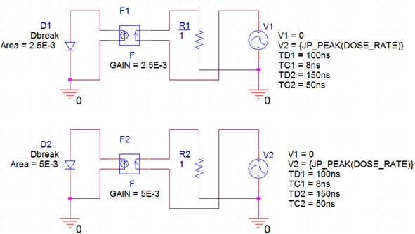
Figure 2: Circuit Design for Dose-Rate effects
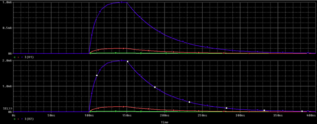
Figure 3: Simulation results for Dose-Rate effects
The simulation results determine the circuit response as a function of dose rate.
Single-Event Upset (SEU) occurs when a high-energy ionizing particle, such as heavy ions, alpha particles or protons, irradiates a circuit or passes through an integrated circuit causing a disruption in the system logic. The most common effects of SEU are logic upsets in high-density digital circuits particularly memories and the registers in microprocessors. Exact upset levels are very difficult to predict because of the complex nature of the physical mechanism involved. However, simulations can aid greatly in evaluating design and process changes to increase the hardness of the circuit to this type of event.
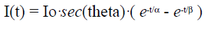
One analysis procedure for SEU is similar to that used for doserate effects discussed earlier. A current generator is inserted in the circuit description to model the charge collected on an assumed susceptible node as a result of the particle hit. The following equation gives an analytical approximation for this current:
where:
Io is approximately the maximum current,
theta is the angle of incidence of the particle to the surface of the circuit,
α is a collection time constant of the junction, and
β is the time constant of initially establishing the ion track.
Io varies according to particle type and is proportional to the energy of the particle and the doping profile of the semiconductor material. The total current increases as the angle of incidence varies from grazing to near normal. The following example demonstrates how PSpice can be used to perform the Analysis of Single Event Upset:
.PARAM IO = 1E-3 ; approximate peak current
.PARAM ANG = 1.3 ; angle of incidence (in radians
.FUNC ISEU(IO,ANG) IO*(EXP(-TIME/150PS)-EXP(-TIME/40PS))/COS(ANG)
.STEP PARAM IO LIST 1E-3 3E-3 1E-2
GSEU 1 1 0 VALUE={ISEU(IO,ANG)}
The .FUNC statement is used to define the SEU current as a function of the peak current, Io, and the incidence angle, ANG. Using the Analog Behavioral Modeling extensions, a current source GSEU is included in the circuit description to represent the charge collected on the susceptible node.
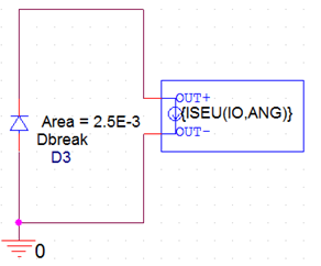
Figure 4: Circuit Design for Single-Event Upset
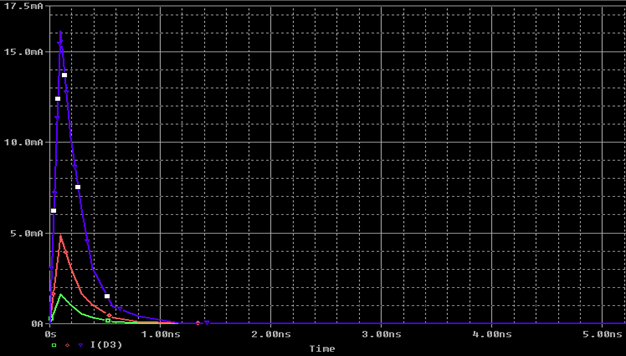
Figure 5: Simulation results for Single-Event Upset
Ionizing radiation produces both transient photocurrents and permanent damage in semiconductor devices. The degree of this permanent damage is proportional to the total accumulated dose and results in a general degradation of device performance.
For example, when MOS structures are exposed to ionizing radiation, they experience a net change in the charge associated with the Si-SiO2 interface. This change in charge has the following two components: (i) the charge stored in the oxide, and (ii) the charge stored in the hole-electron interface traps. The net result is to shift the threshold voltages of both p-channel and n-channel devices toward enhancement mode operation. In addition to this threshold voltage shift, increases in the surface state density produce decreases in surface mobility and a variation in the turn on characteristic of the MOS transistors. The decreased mobility is the result of increased diffusion carrier scattering at the silicon surface. The variation in turn-on characteristics is caused by the filling and emptying of the surface traps as the channel is formed.
Essentially all investigations of the effects of total dose radiation (permanent damage) on semiconductor devices have been made in terms of changes in the device electrical parameters. Analyses on MOS technologies are generally performed as follows:
1. Model parameters are extracted from test devices at several total dose levels over the range of interest.
You must be very careful not to project much outside the range for which experimental data is available, since slight process variations can radically affect the model parameter versus total dose relationship.
2. An analysis of the model parameters is then performed to determine what parameters are most affected by the total dose and then, relationships are developed to describe the shift in the model parameters as a function of total dose.
The following example is given to show the technique. It is assumed that changes in the threshold voltage and mobility are the dominant total dose effects.
.PARAM DOSE = 0.0 ;initialization of total dose
.STEP PARAM DOSE LIST 0 1E5 1E6
.FUNC VTO_DOSE(DOSE) 1.65*(1 - 4.18E-6*DOSE + 2.76E-12*DOSE*DOSE)
.FUNC UO_DOSE(DOSE) 600.0*(1 - 5.00E-7*DOSE)
.MODEL NN2 NMOS ( VTO={VTO_DOSE(DOSE)} UO={UO_DOSE(DOSE)} )
The .STEP capability is used to determine the circuit performance as a function of total dose. Simulations are performed at DOSE = 0.0 (pre-rad), 1E5, and 1E6 rads(Si). Note that the functional relationship between the threshold voltage and total dose has been defined as a nonlinear function, in this case a second order polynomial fit. The variation in mobility as a function of total dose has been assumed to be linear.
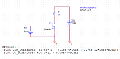
Figure 6: Circuit Design for Total Dose Effects
The following are the simulation results for total dose effects when DOSE=0 [GREEN] , DOSE=1E5 [RED], and DOSE=1E6 [BLUE].
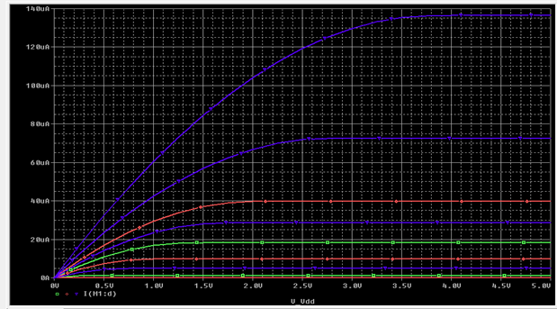
Figure 7: Simulation result when DOSE=0, 1E5, 1E6
[1] J. L. Wirth, S. C. Rogers, “The Transient Response of Transistors and Diodes to Ionizing Radiation,” IEEE Transactions on Nuclear Science, NS-11(5):24-38, November 1964.
[2] Handbook of Modeling for Circuit Analysis Including Radiation Effects, Air Force Weapons Laboratory, AFWLTR- 79-86, Albuquerque, New Mexico, May 1979.
[3] C. G. Messenger, “Collection of Charge on Junction Nodes from Ion Tracks,” IEEE Transactions on Nuclear Science, NS-29(6):2024, December 1982.
© Copyright 2016 Cadence Design Systems, Inc. All rights reserved. Cadence, the Cadence logo, and Spectre are registered trademarks of Cadence Design Systems, Inc. All others are properties of their respective holders.
Copyright © 2020 Cadence Design Systems, Inc. All rights reserved.