Here you will find out latest app notes.
Transmission lines are used to propagate digital and analog signals, and as frequency domain components in microwave design. This app note illustrates the steps and issues involved in modeling and analyzing transmission lines in PSpice.
Transmission lines are used for varied applications, including:
OrCAD PSpice contains distributed and lumped lossy transmission lines that can help to improve the reliability of many applications. For analog and digital circuits, there is a need to examine signal quality for a printed circuit board and cables in a system. For analog circuits, the frequency response of circuits with transmission lines can be analyzed. It is the purpose of this article to examine the steps and issues involved in modeling and analyzing transmission lines in PSpice.
The analysis of transmission line nets requires multiple steps. These steps are given in the following flowchart:
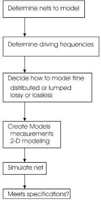
Figure 1. Analysis flowchart for transmission line nets
This article provides information for the two center blocks, by discussing relevant devices and models in PSpice, along with specific modeling techniques and examples.
Concepts
This section presents the basic concepts of characteristic impedance and propagation delay, and reflections and crosstalk.
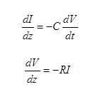
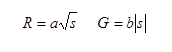
The characteristic impedance of a transmission line is the ratio of the voltage to the current. For a uniform
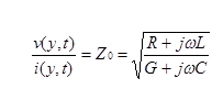
line, it is invariant with respect to time and position on the line:
If R and G are zero, the characteristic impedance will not depend on frequency, and reduces to

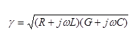
The attenuation constant is the real part of the propagation constant and is important when losses must be considered.
The propagation delay is the reciprocal of the phase velocity multiplied by the length of the transmission line:
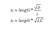
where c is the speed of light, and er is the relative dielectric constant. For a uniform, lossless transmission line.
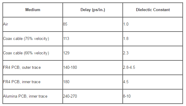
Table 1. Delay And Dielectric Constants For Some Transmission Lines
When a voltage step is traveling down a uniform impedance transmission line, and then encounters an abrupt change in impedance, a portion of the incident energy is “reflected” back. The amount of energy reflected depends on the degree of impedance mismatch. The voltage reflection coefficient, (Z1-Z0)/(Z1+Z0) is a measure of this mismatch:
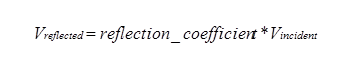
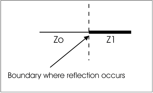
Figure 2. Impedance reflection across a boundary
Crosstalk is undesired energy imparted to a transmission line due to signals in adjacent lines. Crosstalk magnitude is dependent on risetime, signal line geometry and net configuration (type of terminations, etc.).
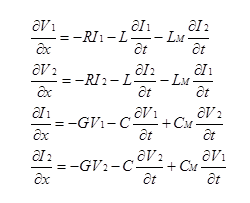
Quantitatively, this energy results from mutual inductances and capacitances in the Telegrapher’s Equations:
Crosstalk is often discussed in terms of forward and backward crosstalk coefficients. These are determined by the ratio of mutual capacitance to self-capacitance, and mutual inductance to self-inductance. If a disturbing line j is coupled to a victim line i that is terminated in its characteristic impedance, these coupling coefficients are
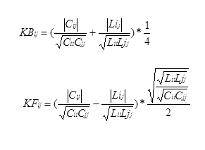
These expressions are valid for loose couplings (KB < 0.25). It is clear that crosstalk can be decreased by decreasing mutual coupling Cij and Lij, or by increasing the coupling to ground.
Figure 3 indicates two signal lines in close proximity that are capacitively coupled (CM) and inductively coupled (LM). Both lines have the same characteristic impedance, Z0, and are fully terminated to avoid reflections. One line is “active” and transmits a pulse, while the other is “passive”.
At the source end of the passive line, the current due to CM and the current due to LM are additive. These summed currents produce a voltage drop of the same polarity as the source voltage, termed “Near End” or “Backward” crosstalk (it travels the opposite direction to the source pulse). At the far end of the passive line, the current due to CM and the current due to LM are of opposite polarity producing “Far End” or “Forward” crosstalk.
Figure 3. Two parallel coupled transmission lines. L=length.
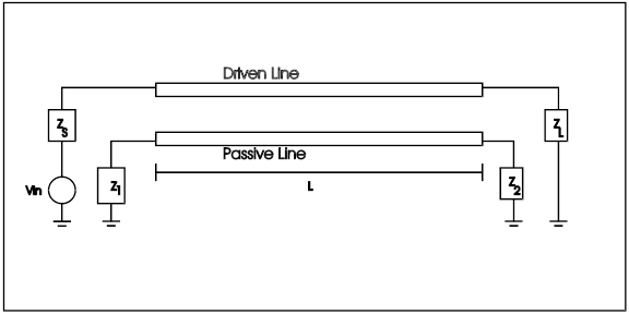
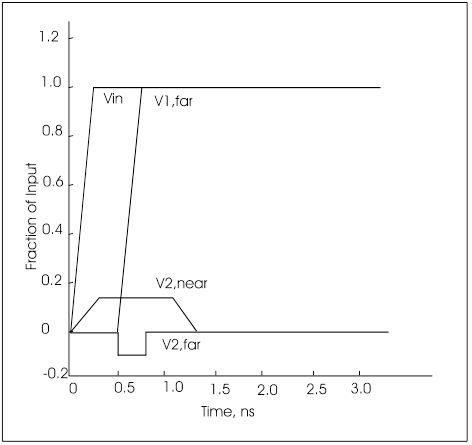
Figure 4. Near and far end crosstalk resulting from a step input on an adjacent line
Defining the point at which an interconnect should be treated as a transmission line and hence reflection analysis applied has no consensus of opinion. A rule of thumb is when the delay from one end to the other is greater than risetime/2, the line is considered electrically long. If the delay is less than risetime/2, the line is electrically short. Hence, the following guidelines:
“Lumped” and “short” lines may always be modeled by lumped circuits. The topic of the next section is to decide how to best model an electrically “long” line.
Ideal and Lossy Transmission Lines
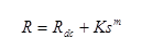
Transmission lines that are lossless, that is R=G=0, are termed ideal transmission lines. This is valid if attenuation and skin effect are either negligible or not of concern for the signal frequencies being analyzed.
For real lines, the series resistance is not quite zero, and the phase velocity is slightly dependent on the applied frequency. These non-idealities result in attenuation and dispersion.
Attenuation results in a reduction in signal amplitude, which may be a function of frequency.
Dispersion results from the propagation velocity being different for the various frequencies.
These effects can cause the frequency components of a signal to be quite different at the far end of the line, compared to the source. The fast rise and fall times of the input signals can be reduced and become “rounded”. It should be noted that there is a theoretical condition where there is attenuation without dispersion, when R/L = G/C. This is normally not of practical significance.
An attenuation vs frequency curve is often provided by cable manufacturers to show susceptibility to these effects:
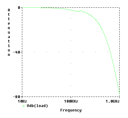
Figure 5 – Attenuation vs. Frequency for a 100 meter lossy coax cable
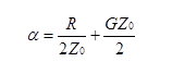
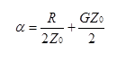
Quantitatively, attenuation is the real part of the complex propagation constant
At high frequencies the real part is
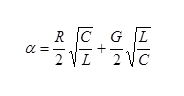
or
The following sections discuss the physical causes of line loss, skin effect, dielectric loss, and proximity effect.
Skin effect results from the fact that currents tend to concentrate on the conductor surface. Current density continuously increases from the conductor center to its surface. For classical skin effects, the penetration depth is given by
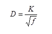
where K=1/sqrt(p*m*s), m=magnetic permeability of the conducting material expressed in henries per unit length, and s=conductivity of the conducting material. For SI units and for a copper conductor s=5.85x10⁷ (ohm-meter)-1 and m=4p×10-7 (H/meter).
The skin effect reduces the equivalent conductor cross-sectional area, which causes the effective resistance per unit length to increase with increasing frequency.
Dielectric losses result from leakage currents through the dielectric material, which causes an increase in the shunt conductance per unit length. This results in signal attenuation. For frequencies below 250 MHz, this loss can usually be neglected. Skin effect losses will dominate up through RF frequencies.
This is a current density redistribution in a conductor due to the mutual repulsion (or attraction) to currents flowing in nearby conductors. This current density redistribution reduces the effective cross-sectional area of the conductor, thereby increasing the series resistance. No general rules of thumb have been proposed due to its complicated nature. This effect is a function of the conductor diameters, separation of conductors, and frequency.
Influence of Loss Effects on Primary Line Parameters
For coaxial lines, skin effect losses dominate and the resistance per unit length is described by
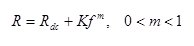
At high frequencies Rdc can often be neglected
It has been shown for 2-wire lines (twisted pair, parallel wire) that, as the frequency is increased, the skin effect and proximity effect cause a slight reduction in the effective per-unit length self-inductance of the line. This frequency effect can often be neglected in models, and can lead to non-causality.
This depends primarily on the dielectric constant of the insulating medium and the geometry of the conductor. Capacitance per unit length is constant over a wide range of frequencies for most dielectrics, such as Polyethylene.
If the loss tangent is available, G may be modeled by use of
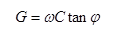
Where C is capacitance per unit length, w is the angular frequency, and tanj is a dielectric material coefficient known as the “loss tangent”.
It is often necessary to obtain R and G simultaneously from the attenuation vs. frequency curve. The following methods have been used successfully:
1: Using two points at the lower and upper bound of the signal frequencies of interest, simultaneously solve two equations of the form:
2: Attribute 90% of the loss to R, and 10% of the loss to G [3]. The rational for this is that most of the loss at high frequencies comes from the resistance of the center conductor.
Specific examples of modeling the attenuation curve are given later.
Both ideal and lossy transmission lines may be modeled as either distributed or lumped. The internal transmission line device in PSpice is distributed, but often a lumped macromodel can be used to advantage. For this reason both are provided in OrCAD’s libraries. The following are guidelines for model selection.
Model Selection
Networks of transmission lines will typically span multiple categories. Each transmission line should be modeled as simply as possible, for faster simulation speed.
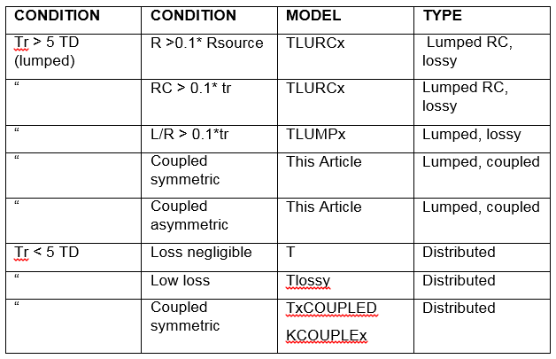
Table 2. Model Selection For Different Rise Time And Primary Line Constants.
Distributed (T and TLOSSY)
OrCAD provides both ideal and lossy distributed models:
The parameters of the ideal transmission line are:
The parameters of the lossy transmission line are:
Lumped RC models (TLURCx)
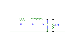
An RC line is a special case where R/L is large (or the series inductance is small). The simplest model for an RC line is a capacitor and a resistor.
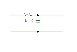
Figure 6. Single RC Lump.
OrCAD provides the following RC lumped models in the transmission line library:
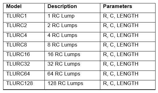
Table 3. RC Lumped models.
For TLURC64, the value of R for one lump is R*LENGTH/64.
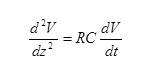
A distributed RC line can be realized with a cascade of T-sections, each T like that of figure 6. If the number of sections were infinite, the governing equations would be
These combine to produce the diffusion equation
The “Elmore delay” of this line is td=0.5 R CL2 + R CL*L + Rd*CL + Rd CL, where Rd is the driver resistance, CL is the load capacitance, and L is the line length. PSpice can be used to predict this delay for heterogeneous networks.
When wL/R>>1 or wC/G>>1, the per unit length inductance should be included in the lumped model.
OrCAD provides the following RLCG lumped models in the transmission line library
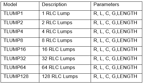
Table 4. RLC Lumped models.
Transmission Line Couplings
Transmission lines may be coupled to study the effects of mutual inductive and capacitive coupling, such as crosstalk. It is possible to use both a distributed and a lumped model for these macromodels.
Systems of coupled transmission lines can be described by their capacitance and inductance matrices. The elements of the capacitance matrix C are defined by
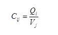
Cij gives the charge induced on the ith conductor when conductor j is set to a potential of 1 Volt, and all other conductors are grounded. The diagonal elements of C are related to the capacitance of the ith conductor to ground by the following formula
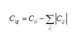
Off diagonal elements are the mutual capacitances for conductors i and j.
Terms of the inductance matrix L are described by
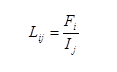
Lij gives the flux between the ith conductor and the ground plan when conductor j carries 1.0 Amp, and all other conductors are floating. Off diagonal terms are mutual inductances.
In PSpice, the mutual parameters of a coupled transmission line structure are:
LM - Mutual inductance between adjacent tlines per unit length
CM - Mutual capacitance between adjacent tlines per unit length
The methods of [1] and [2] are used to decouple the transmission line parameters, subject to the following assumptions:
Edge effects are neglected as a result of the first limitation.
The following models are available for coupled transmission lines:
Table 5. Transmission line coupling parts.
In some cases it is desirable to use a lumped circuit to model coupling. Here we present a symmetric, coupled, 3 conductor, lumped model:
* symmetric coupled 3 conductor lumped
.subckt C3L in1 in2 in3 out1 out2 out3
+params: len=1 r=0 l=1 c=1 lm=1 cm=1
* first conductor
r1 in1 1 {len*r+1u}
l1 1 2 {len*l/2}
c1 2 0 {len*c}
l2 2 out1 {len*l/2}
* second conductor
r3 in2 3 {len*r+1u}
l3 3 4 {len*l/2}
c2 4 0 {len*c}
l4 4 out2 {len*l/2}
* third conductor
r5 in3 5 {len*r+1u}
l5 5 6 {len*l/2}
c3 6 0 {len*c}
l6 6 out3 {len*l/2}
*mutual couplings
k1 l1 l3 {lm/l}
k2 l2 l4 {lm/l}
k3 l3 l5 {lm/l}
k4 l4 l6 {lm/l}
k5 l1 l5 {lm/l}
k6 l2 l6 {lm/l}
c4 2 4 {len*cm}
c5 4 6 {len*cm}
c6 2 6 {len*cm}
.ends
This model can be extrapolated to two, four, and five conductors.
To be able to decouple the inductance and capacitance matrices, LM < L and CM < C. Large values of LM can lead to a negative eigenvalue when decoupling the matrix.
Rules Of Thumb For Choosing Between Lumped And Distributed Types
Library Models And Modeling
This section provides an overview of available models and presents modeling techniques and considerations.
Library Models
OrCAD's libraries (PSpice A/D and PSpice) contain lossy transmission lines for coax and twisted pair (frequency domain analysis only), as well as other distributed and lumped macromodels.
Coax Modeling
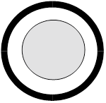
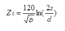
A simple for formula for the characteristic impedance of coax is
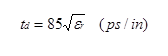
Where d1 is the diameter of the inner conductor, and d2 is the diameter of the inside surface of the shield. The propagation delay is
For coaxial lines, the primary loss is from the skin effect. The resistance per unit length becomes:
Where 0 < m < 1. For coax inductance and capacitance per unit length can be treated as frequency independent. Conductance per unit length is
Where C is capacitance per unit length, w is the angular frequency, and tanf is a dielectric material coefficient (“loss tangent”). The angle f is called the dielectric loss angle. This angle is usually quite small (<0.005 radians) for most dielectrics up to RF frequencies.
The following is an example model of RG6A/U coax from OrCAD’s libraries. Note that R and G use the Laplace variable ‘s’ to model attenuation as a function of frequency:
* Model parameter units are as follows:
* len: meters
* r: Ohms/meter
* l: Henries/meter
* g: Mhos/meter
* c: Farads/meter
*$
* Z0(Ohms) vp(%) F1(MHz) Loss1(dB/100Ft) F2(MHz) Loss2(dB/100Ft)
* RG6A/U 75 66 100 2.9 1000 11
.model RG6A/U TRN (r={59.5022u*sqrt(2*s)} l=379.050n
+ g={0.0428900p*abs(s)} c=67.3867p)
*$
An alternate version of the model is obtained by using the FREQ attribute on the RG6A/U part to use a specified frequency to evaluate R and G. This can have some advantages in transient analysis.
* Subckt version uses fixed frequency, frq, to model simple lossy line
*
* Near end hi
* | Near end lo
* | | Far end hi
* | | | Far end lo
* | | | |
.subckt RG6A/U A1 A2 B1 B2 params: frq=100Meg len=1
.param PI2 {3.141592654*2}
.model RG6A/U TRN (r={59.5022u*sqrt(PI2*frq)} l=379.050n
+ g={0.0428900p*PI2*frq} c=67.3867p)
t A1 A2 B1 B2 rg6a/u len={len}
.ends
Attenuation vs. frequency data is generally available to ~1GHz for coax cable. At frequencies above ~1MHz, R and G have the following dependencies on frequency:
Here is complex frequency (the Laplace variable).
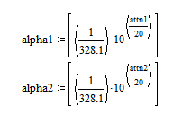
Modeling Attenuation In Mathcad:
The following is a Mathcad program which fits the loss parameters R and G to two points of the Attenuation vs. Frequency curve:
Enter attenuation of 100' of cable in dB at f1.
attn1 :=2.9
Enter characteristic impedance of cable.
Enter frequency @ attn1

Enter attenuation of 100' of cable in dB at f2.
attn2 :=11
Enter frequency @ attn2
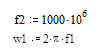
F1 in radians/sec

F1 in radians/sec
Attenuation factor for f1 in nepers/meter
Attenuation factor for f2 in nepers/meter
alpha1 = 0.0042559231
alpha2 = 0.0108141844
* r and g are both functions of frequency, and are computed using the method
* described in "Transmission Lines" by Robert Chipman, McGraw-Hill, 1968,
* pp 65-66. r is assumed to increase in proportion to the square root
* of frequency, while g varies in direct proportion to frequency. A high
* frequency relationship for the attenuation factor is:
*
* alpha = ((r / z0) + (g * z0)) / 2,
*
* and r and g can be found by selecting values of alpha at two frequencies
* (100 MHz and 1 GHz are used here) and solving two simultaneous equations:
*
* alpha1 = (.5 / z0) * r1 + (.5 * z0) * g1
* alpha2 = (.5 / z0) * sqrt(w2 / w1) * r1 + (.5 * z0) * (w2 / w1) * g1
*
* The alpha's are converted to units of nepers per meter, and the frequencies
* (w1 and w2) are in units of radians per second. Kramer's rule gives:
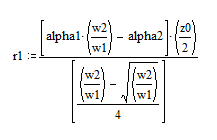
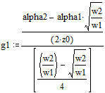
r1 = 0.6963951914
g1 = -0.0000103123
* Then the frequency-dependent expressions for r and g are:
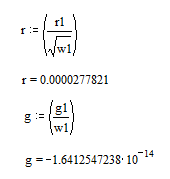
The transmission line parameters derived are then
R={2.77821e-5*sqrt(s)}
G={-1.64125e-14*abs(s)}
Twinax and Shielded Twisted Pair (STP) Modeling
Twisted shielded pair (STP) or “twinax” is recommended for differential transmission systems at high frequencies or in noisy environments. Although it has superior noise rejection, the proximity of the shield increases the distributed capacitance which significantly attenuates the signal.
To model STP for differential driving, a multiconductor transmission line is needed.
A simple for formula for the characteristic impedance of two parallel wires is
Where d is the diameter of the conductor, and s is the separation between wire centers. The propagation delay is
For multiconductor (crosstalk) simulations, it is important to obtain the conductor to conductor coupling parameters LM and CM. Here are suggestions for obtaining these parameters:
Sometimes odd and even mode impedances are provided rather than the inductance and capacitance matrices. The even and odd mode characteristic impedances are related to L, C, LM and CM in the following way:
Zoe = SQRT((L + e*LM)/(C - e*CM))
Zoo = SQRT((L + o*LM)/(C - o*CM))
Tde = SQRT((L + e*LM)(C - e*CM))
Tdo = SQRT((L + o*LM)(C - o*CM))
Zoe and Zoo are the even and odd mode impedances, respectively, and Tde and
Tdo are the corresponding delays. The coefficients e and o are the even and
odd mode eigenvalues of the matrix [L][C], and come out to e=SQRT(2)/2 and
o=-SQRT(2)/2 for two symmetric lines.
L, C, Lm and Cm are found by solving the 4 equations above in terms of Zoe, Zoo,
Tde, and Tdo.
Twinax attenuation curves have an a + b*sqrt(f) frequency dependence, similar to coax. The same method as suggested for coax may be used to model R and G for twinax.
Unshielded Twisted Pair (UTP) Modeling
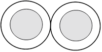
Unshielded twisted pair (UTP) can not be used at higher frequencies, as can STP.
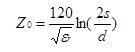
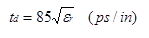
A simple for formula for the characteristic impedance of two parallel wires is
Where d is the diameter of the conductor, and s is the separation between wire centers. The propagation delay is
For UTP, the inductance in the region below ~500KHz can vary slightly with frequency. The distributed lossy transmission line model allows R and G to depend on frequency, but not L. The best solution is to pick the value of L for the frequencies of interest.
OrCAD's transmission line library contains four UTP models:
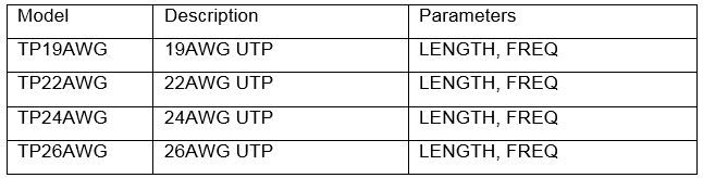
Table 6. UTP models in the transmission line library.
Note: These models can be used for transient analysis by setting FREQ=<signal frequency>. This will allow PSpice to use the R, G, and L values corresponding to <signal frequency>. For use with AC sweep, set FREQ=<nothing>.
Attenuation curve data is generally not available above ~16MHz for UTP cable. At these mid-range frequencies, attenuation does not always obey a square root dependence on frequency. Here is a suggested method to model UTP attenuation:
Use a linear least square fitting routine to fit more points of the attenuation curve to a polynomial of the form

Where s is complex frequency.
Geometry Parameterized Models
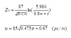
Another way to model a transmission line is by describing its physical dimensions, and relative dielectric constant. There are empirical equations derived for many popular transmission line geometries [6]. The functions supported by PSpice’s analog behavioral modeling expressions allow models to be created for a large variety of geometries, including coaxial, paired, coplanar, microstrip, stripline, inverted microstrip, and low order modes of waveguides. Coupled lines may also be parameterized by their geometry. Two of the most common types are microstrip and stripline.
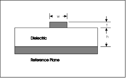
Figure 8. Microstrip configuration.
Simple formula valid for 0.1<w/h<2.0:
Here h is the height above ground, w is the trace width, and t is the line thickness.
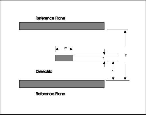
Figure 9. Stripline configuration.
Simple formula:
Here h is the separation between grounds, w is the trace width, and t is the line thickness.
A library of geometry parametrized models is available and can be downloaded from ftp.microsim.com/tech_support/tlinean.zip.
Ribbon Cable Multiconductor Modeling
This type of cable is most used for single ended data transmission, is familiar to designers and can consist of any number of conductors. Ribbon cable is very flexible because it is narrow, and can fit in thin spaces where round multiconductor cable would not. Grounds can be used as “barriers” between asynchronous signals.
A simple for formula for the characteristic impedance of two parallel wires is
Where d is the diameter of the conductor, and s is the separation between wire centers. The propagation delay is
For multiconductor (crosstalk) simulations, it is important to obtain the conductor to conductor coupling parameters LM and CM. Here are suggestions for obtaining these parameters:
Measure the capacitance and inductance matrices in the lab.
Use a 2-D field solver, such as the code provided in [5].
Round Multiconductor Cable Considerations
Round multiconductor cable is generally discouraged for high-speed applications because the worst case amount of crosstalk that may occur varies from cable to cable. Yet, statistical analysis of crosstalk can be performed for cables meeting tight manufacturing specifications. If a known minimum distance between two sensitive conductors along with a maximum parallel length can be determined, then the resulting crosstalk can be studied.
Best bets for obtaining the inductance and capacitances matrices are:
This example serves to illustrate the process of modeling and simulating a high-speed system clock net, by applying the steps outlined in the flowchart.
Introduction
A ECL system clock must pass through multiple PCBs (including backplanes), and a 30 ft cable. It is desired that ribbon cable be used, but if necessary twinax can be used (although it is more expensive).
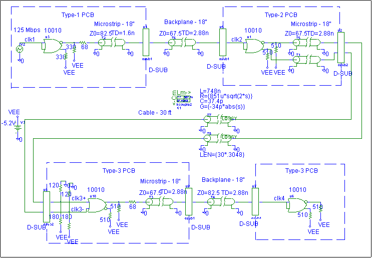
Figure 11. ECL system clock spanning multiple PCBs.
STEP 1: Determine driving frequencies and technology constraints.
We are using ECL100K technology, which has the following device characteristics:
Voh=-0.9 volts
Vol = -1.7 volts
High level, 125 millivolts
Low level, 125 millivolts
Although these are guaranteed minimums, each is generally better by about 75 millivolts.
|
Z0 (ohms) |
Fanout=1 (3.3pF) MAX IN. |
Fanout=2 (6.6pF) MAX IN. |
Fanout=4 (13.2pF) MAX IN. |
Fanout=8 (26.4pF) MAX IN. |
|
50 |
1.6 |
1.1 |
0.7 |
0.6 |
|
68 |
1.4 |
0.8 |
0.5 |
0.4 |
|
75 |
1.3 |
0.8 |
0.4 |
0.3 |
Table 7. Maximum open line length for ECL 100K for microstrip.
In practice, there is a tradeoff between use of terminations and lowering power dissipation. Thus, terminations are not perfect in the clock path.
STEP 2: Decide how to model the net.
The data path involves single-ended signals on the PCBs, and a differential signal through the 30 ft ribbon cable. The following are also suggested by the schematic:
STEP 3: Create Models.
These are included in OrCAD’s standard libraries.
The specifications for the ribbon cable are:
Wire radius (mils) = 7.5
Insulation thickness (mils) = 10.0
Relative dielectric constant of insulation = 3.5
Adjacent wire separation (mils) = 50.0
The L and C matrices are obtained from the 2-D code in [3].
L11=0.74850 uH/m
L12=0.5077 uH/m
L22=0.74850 uH/m
C11=37.432 pF/m
C12=18.716 pF/m
C22=37.432 pF/m
Attenuation curves have been fitted to R and G:
R={851u*sqrt(2*s)} ohms/m
G={-0.340p*abs(s)} siemens-m
L11=L22=332.730 nH/m
C11=C22=57.02 pF/m
L12=253.85 nH/m
C12=45.131 pF/m
R={241.315u*sqrt(2*s)} ohms/m
G={-0.140442p*abs(s)} siemens-m
This cable is better matched to the PCBs, but is more expensive.
The ECL clock will be routed on an outer layer of a PCB (microstrip) with the following properties:
An impedance of 75+/-10 ohms will be used. The propagation delay is 0.16 ns/in. Simulations should investigate the effect of the upper ends of the tolerance range.
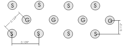
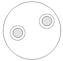
Figure 11. Signal/Ground arrangement in D-SUB connectors; S=signal, G=ground.
We use a 2-D finite-element field solver to obtain the capacitance and inductance matrix:
L11=2.97 nH
L12=0.98 nH
L22=2.91 nH
C11=0.122 pF
C12=0.0314 pF
C22=0.122 pF
An 8 Lump RLCG model can be used such as TLUMP8. For simulation of crosstalk we can use KCOUPLE2 or a lumped coupled model.
STEP 4: Simulate Net. Run a 150 ns transient analysis for the circuit of figure nn.
STEP 5: Compare results to design specifications.
It is extremely important for a system clock to meet the specifications for Vil,max and Vih,min at all receiver inputs. If a “glitch” were to exceed these voltages, we risk the possibility of data corruption.
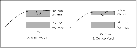
Figure 12. Voltage margins
The Probe plot (figure 13) shows that Vih,min=-1.165mV and Vil,max=-1.475mVare never exceeded, and the clock edges are monotonic through the transition region. The differential input voltage at the end of the 30 ft cable is 382mV worst case, which exceeds the required minimum 300mV.
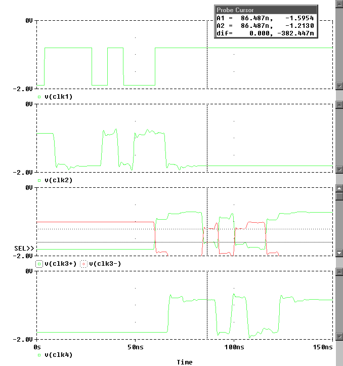
Figure 14. OrCAD Probe plot showing clock signals at the inputs of the receivers
Resolution of the Impulse Response
For frequency independent R and G, OrCAD PSpice calculates closed form impulse responses [1]. But, when R and G are Laplace expressions, a numerical impulse response is calculated using FFT. The minimum number of points for the FFT is 256 and the maximum is 65536. Decreasing RELTOL will increase this frequency resolution.
Here are some points to keep in mind:
WARNING – G/C for T_T1 is 1e+015. Results may be inaccurate for G/C > 1e10.
For these high loss lines, use a lumped modeling approach as discussed previously.
Example: 10 m of RG58/U coax is used for a 60ns and 600ns simulation. The impulse response is ~4% non-causal, but the results are still valid. The 60ns simulation shows good resolution at far end of line, however, the 600ns simulation requires setting RELTOL=0.0001 to obtain the same good resolution.
Non-Causality And The Numerical Impulse Response
PSpice uses a numerical convolution to obtain the impulse responses for lossy transmission lines with frequency dependent losses. It is an assumption fundamental to the convolution method [1] that the impulse response is a causal function of time. Unfortunately, not all Laplace expressions have causal impulse responses.
If an impulse response is partially non-causal, PSpice will write a message to the output file:
WARNING -- 10.9038 percent of T_T1 impulse response is non-causal.
WARNING -- It should be delayed by at least 4.86374e-013 sec.
Non-causality more than a few percent can lead to highly inaccurate results, depending on what feature of the impulse response has been lost through truncating values for t<0. The following are guidelines for improving the simulations.
REFERENCES
[1] Roychowdhury, J.S. and D.O. Pederson, “Efficient Transient Simulation of Lossy Interconnect”, 28th ACM/IEEE Design Automation Conference, 1991, pp. 740-745.
[2] Tripathi, V.K., and J.B. Rettig, “A SPICE Mode for Multiple Coupled Microstrips and other Transmission Lines”, IEEE MTT-S Digest, 1985, pp. 703-706.
[3] Banzhaf, W., “Simulating Lossy Transmission Lines With PSpice”, RF Design, January 1993, pp. 25-27.
[4] Cooper Industries, Belden Wire and Cable Master Catalog, 1996.
[5] Paul , C.R., Analysis of Multiconductor Transmission Lines, Wiley Series in Microwave and Optical Engineering, K. Chang (Ed.), John Wiley & Sons, Inc., 1994.
[6] Wadell, B.C., Transmission Line Design Handbook, Artech House, 1991.
[7] National Semiconductor, F100K ECL 300 Series Databook and Design Guide, 1992.
[8] Johnson , H.W. and M. Graham, High-Speed Digital Design: A Handbook of Black Magic”, Prentice Hall PTR, 1993.
[9] Deutsch et. al., A., “High-speed signal propagation on lossy transmission lines”, IBM J. Res. Dev., Vol. 34, No. 4, pp. 601-615, July 1990.
© Copyright 2016 Cadence Design Systems, Inc. All rights reserved. Cadence, the Cadence logo, and Spectre are registered trademarks of Cadence Design Systems, Inc. All others are properties of their respective holders.
1766 12/13 CY/DM/PDF
Copyright © 2020 Cadence Design Systems, Inc. All rights reserved.