
Hello Everyone,
I was trying to simulate a simple AND Gate circuit in .CIR file
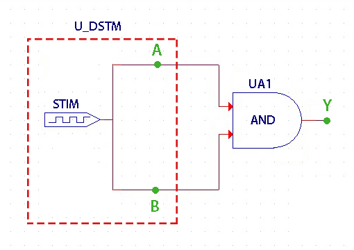
Circuit Diagram is as follows:
My Source Code is as follows:
AND Gate Simulation with propagation delay=0.5ms
.lib "C:\Cadence\SPB_16.6\tools\pspice\library\dig_io.lib"
U_DSTM STIM(2,11) $G_DPWR $G_DGND
+ A B ;Node Names
+ IO_STM IO_LEVEL=0
+ 0s 00
+ 1ms 01
+ 2ms 10
+ 3ms 11
UA1 AND(2) $G_DPWR $G_DGND A B Y
+ T_AND2 IO_STD
.MODEL T_AND2 UGATE
+ TPLHMN=500015ns TPLHTY=500020ns TPLHMX=500025ns
+ TPHLMN=500015ns TPHLTY=500020ns TPHLMX=500025ns
+)
.TRAN 1ms 4ms
.PROBE D(A) D(B) D(Y)
.END
Now the probe plot for the above source code is:
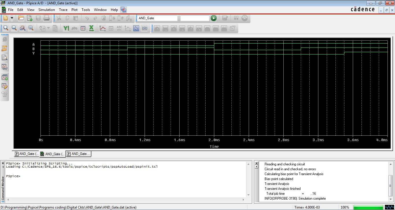
In the plot, we can see many of y-axis space is unoccupied,
so how can i scale the plot so that most of the portion is filled with the waveform,
i.e., how can i increase the size of A , B and Y waveforms in the plot?
Copyright © 2020 Cadence Design Systems, Inc. All rights reserved.
Thank you for sharing this rate, very helpful info. wuxiaworld