PSpice A/D

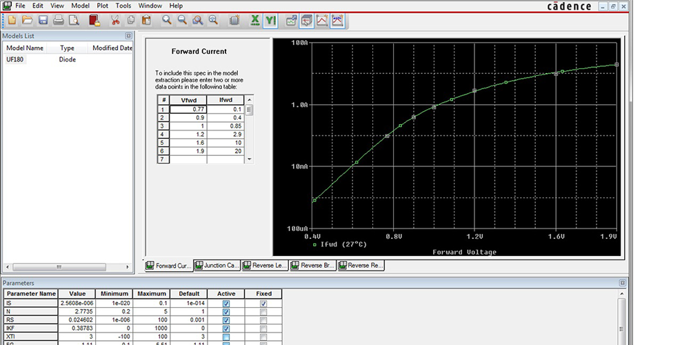
Cadence® PSpice® A/D is a full featured analog circuit simulator with support for digital elements. It integrates easily with Cadence PCB schematic entry solutions and comes with an easy-to-use graphical user interface that equips the user with the complete design process to help solve virtually any design challenge from high-frequency systems to low-power IC designs. Due to its wide popularity PSpice models with built-in mathematical functions and behavioral modeling techniques are available from many IC vendors.

Overview

PSpice A/D Overview

PSpice® A/D Simulation Technology enables engineers to :  

Understand and explore circuit performance and functional relationships with “what if” scenarios and design analysis

• Simulate complex mixed-signal designs, containing both analog and digital parts to support models like IGBTs, pulse width modulators, DACs, and ADCs

​Download PSpice@ A/D datasheet

PSpice A/D Technology Highlights

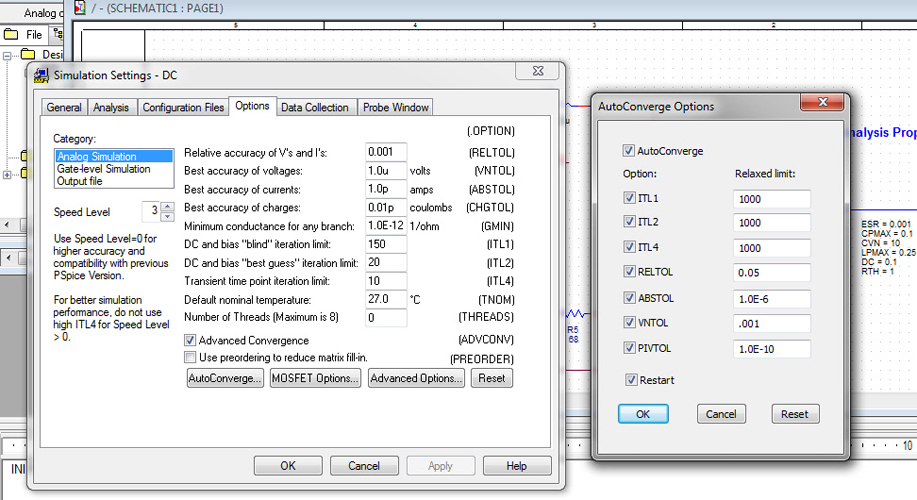
•  Improves simulation times, reliability and convergence for large designs

•  Improves speed without loss of accuracy via integrated analog and event-driven digital simulations

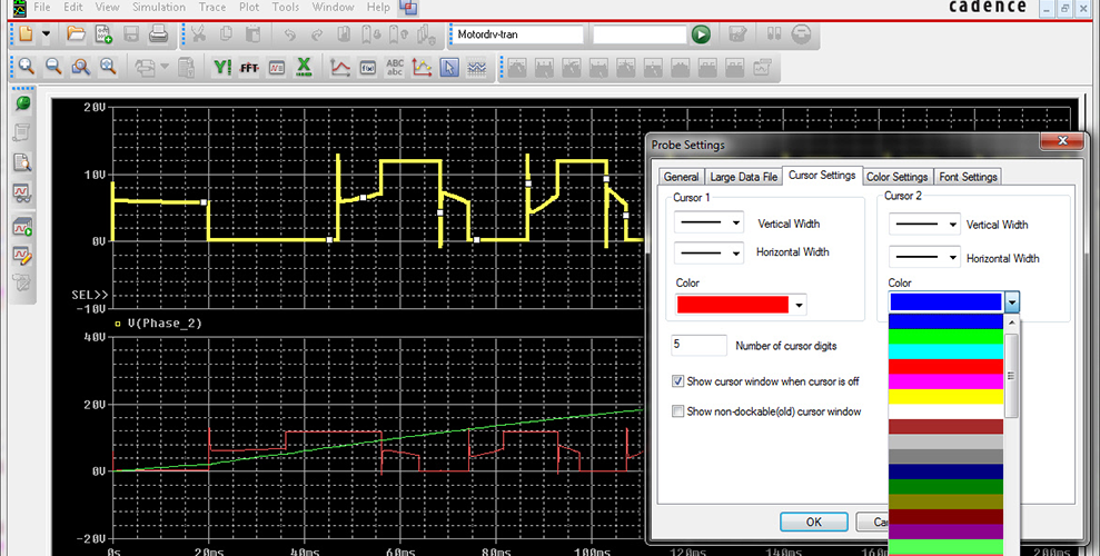
•  Explores circuit behavior using basic DC, AC, noise and transient analysis

•  Allows system-level interfaces to be integrated with electrical designs using the PSpice® Systems Option. View the video

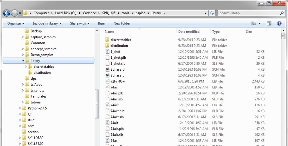
•  Library selection of 33,000+ analog and mixed-signal models

•  Allows for automatic identification of analog and digital signals and automatically applies A-to-D and D-to-A interfaces

•  Allows designers to explore design relationships with “what if” scenarios before committing to hardware

•  Enables designers to identify and simulate functional blocks of complex circuitry using mathematical expressions, functions and behavioral devices


Features

  • Mixed Analog / Digital Simulation
    Mixed Analog / Digital Simulation

    Unified design environment for PCB design and simulations made available by the seamless integration of PSpice® A/ D and Cadence front end PCB design. Get access to large database of more than 33,000 symbols and models for simulation to design with Cadence PCB schematic design entry tool.

    • Set up and run simulations and cross-probe simulation results from OrCAD Capture. View simulation bias results directly on the schematic including node voltages, pin and sub-circuit currents and device power calculations.
    • Use the hierarchical netlister with parametric sub-circuits for faster netlisting of complex hierarchical designs
    • Expanded simulations can be run in the background while design editing continues
    • Create multiple simulation profiles and save them in the OrCAD Capture Project Manager allowing previous simulations to be recalled and run
    • Seamlessly transition between simulations and the schematic design entry tool. 
  • Simulation Environment
    Simulation Environment

    The unified simulation environment provides the ability to :

    • Perform and monitor simulations, view and edit text files, view simulation messages and graphical results.
    • Utilize analog analysis capabilities such as user-defined accuracy, automatic time-step control and proprietary convergence algorithms to control the simulation process
    • Interactively trade off accuracy and simulation time by loosening tolerances and time steps during non-critical periods of transient analysis or by extending a transient analysis beyond pre-specified end time
    • Preempt the current simulation to immediately run another one then return to complete the preempted simulation later; control the queue of simulations waiting to be performed
  • Debugging and Convergence
    Debugging and Convergence

    Debugging and Convergence capabilities include

    • CHECKPOINT RESTART: Save time by storing simulation states at various time-points and then restart simulations from any of the simulation states. You can modify simulation settings and design parameters before starting a simulation from pre-recorded time-state.
    • AUTO-CONVERGENCE: Automatically change tolerance convergence limits to make the design converge. You can use this option to get convergence and then fine-tune simulations by further modifying simulator options. This option is recommended for power electronic designs.
    • ASSERTIONS: Use special parts to insert error and warning conditions for the simulator to flag the conditions as the simulation progresses.
  • PSpice Probe
    PSpice Probe

    PSpice Probe allows users to choose from an expanded set of mathematical functions to apply to simulation output variables.

    • View simulation results in multiple waveform windows
    • Select waveforms by name or by marking a net, pin or part in the schematic
    • Utilize cross-probing markers once and they stay with the analysis as you change and re-simulate the design the marked waveforms appear after each simulation
    • View continuous, real-time “marching waveforms” as simulation progresses
    • Copy and paste high-resolution, scalable waveforms into other applications for producing documentation
    • Create plot window templates and use them to easily plot complex functions of signals, just by placing markers on desired pins, nets and parts in the schematic
    • Measure performance characteristics of your circuit using built-in measurement functions or create your own measurements
  • Built-in Models
    Built-in Models

    Large variety of built-in models adds flexibility to simulations most include temperature effects

    Shipped models include R, L, C, plus:

    • Built-in IGBTs
    • Several MOSFET models including industry-standard BSIM4, BSIM3v3 and the new EKV2.6 model
    • Five GaAsFET transistor models including Parker-Skellern and TriQuint TOM3 models
    • BJT models including Gummel Poon and Mextram
    • Nonlinear magnetic models complete with saturation and hysteresis
    • Transmission line models that incorporate delay, reflection, loss, dispersion and crosstalk
    • Digital primitives including bidirectional transfer gates with analog I/O models
  • Models and Modeling
    Models and Modeling

    Large library of analog and mixed-signal models including parameterized models and a Device Equations Developer’s Kit (DEDK) for implementation of new and custom internal model equations.

    • Select from more than 33,000 analog and mixed-signal models of industry devices
    • More than 4,500 parameterized models for BJTs, JFETs, MOSFETs, IGBTs, SCRs, magnetic cores and toroids, power diodes and bridges, operational amplifiers, optocouplers, regulators, PWM controllers, multipliers, timers, and sample-and-holds. These models allow passing simulation parameters as properties from the Schematic Editor
    • Access basic components plus a variety of macro-models for more complex devices, including operational amplifiers, comparators, regulators, optocouplers, ADCs and DACs
    • Use state space average models to do fast feasibility simulations and control loop analysis for switched mode power supplies
    • Automatically generate OrCAD Capture parts for the models created by the Model Editor

PSpice A/D Videos

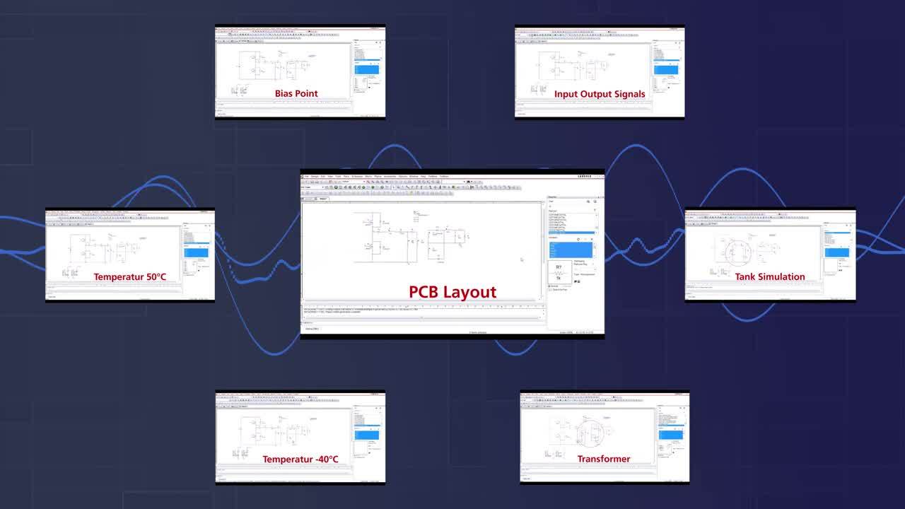
Watch videos to see how to use PSpice® A/D to deliver a complete circuit simulation and verification that meets your changing simulation needs.

A PSpice® A/D Application-Balanced load in a star connection

Watch this 2 mins video and learn more about the behavior of balanced loads in a star connection.

A PSpice® A/D Application-Boost Converter

This video is about the structure and operation of a boost converter, and how such a step-up converter works in principle, illustrated with PSpice technology.

A PSpice® A/D Application-Virtual Prototyping

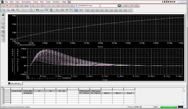
Learn how PSpice® A/D makes virtual prototyping extremely easy and convenient.

A PSpice® A/D Application-Inverting Schmitt Trigger

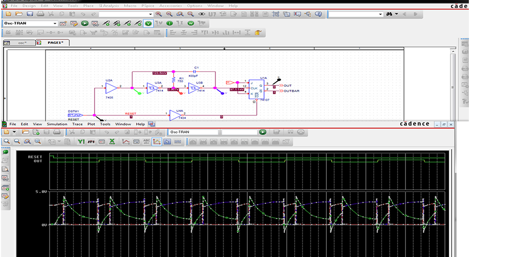
This video is about an important basic circuit of electronics—Inverting Schmitt Trigger.

A PSpice® A/D Application-Bipolar Transistor as a Switch

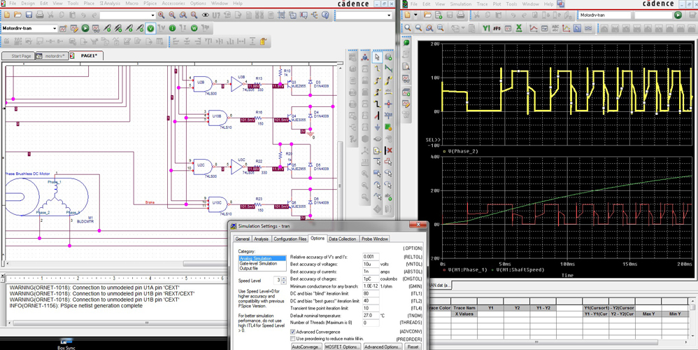
A bipolar transistor functioning as a switch is another basic circuit often used in electronics.

A PSpice® A/D Application-Open Collector Output

Many integrated circuits for digital applications have an open-collector output. In this PSpice tutorial we’ll analyze the behavior and dimensioning of such an open-collector output.

A PSpice® A/D Application-Digital-to-Analog Converter

This video is about the basic structure of a digital-to-analog converter DAC.

A PSpice® A/D Application-Monte Carlo Application

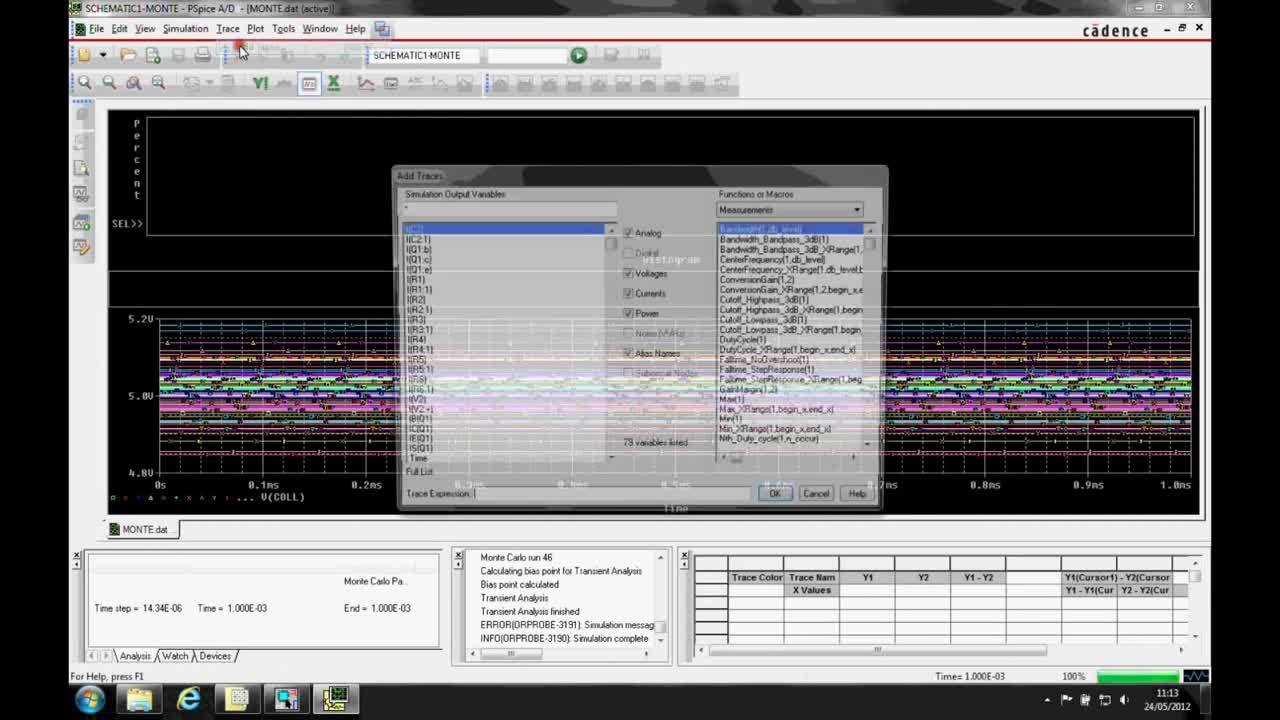
The video provides a Monte Carlo simulation to evaluate the performance of a common emitter amplifier

What’s New


left-image.jpg

PSpice 17.2-2016 Release New Features:

- Virtual prototyping
- 64 Bit simulation engine and result analysis
- New functions for behavioral models 
- TinySwitch-III and Optocoupler device models
- Support for TCL 8.6 
Learn More

PSpice Free Trial


right-image.jpg


OrCAD®/PSpice® software will let you experience all the features and functionalities of the actual software. Download now and discover how easy it is to use the state-of-the-art PSpice technologies.

Download

Have Questions

Join PSpice A/D Forum!

Join Now

Want to Buy PSpice?

Find an OrCAD Channel Partner!

Contact Us
Cadence