Here you will find out latest app notes.
In this application note, we will model potentiometers and variable resistors using OrCAD Capture and simulate the example circuits, which include models of potientiometer and variable resistors, using PSpice.
Electrically, a potentiometer consists of two resistors connected in series. The specification for the potentiometer consists of:
1. The total resistance (R), and
2. The pot’s setting (SET). That is, where the center tap is set.
A convenient way to describe this is to define SET to be 0 when the tap is all the way at the bottom and 1 when it is all the way at the top.
A potentiometer can be implemented by the following subcircuit:
.SUBCKT POT 1 T 2 PARAMS: VALUE=1K SET=0.5
RT 1 T {VALUE*(1-SET)+.001}
RB T 2 {VALUE*SET+.001}
.ENDS
The values 1.001 (instead of 1) and .001 (instead of 0) are used to prevent the resistors from having 0 ohms at the extremes.
So far, the setting of the pot has been static. That is, it does not change with time. This is appropriate for almost all applications, since the time required for the movement of the pot is much longer than the electrical time constants of the circuit. In other words, there is no loss of information by running several transient analyses and varying the pot’s setting with a .STEP command. A typical usage would be:
.PARAM SET=.5
.STEP PARAM(SET) 0, 1, .2
X1 3 5 17 POT PARAMS: R=10K SET={SET}
Here a 10k pot is used in 6 runs, having the settings 0, .2, .4, .6, .8, and 1. In schematics there is a symbol for a potentiometer located in breakout.olb. The following example circuit shows that how a pot may be used with an adjustable regulator.
Note: The pot R1 is swept to show the adjustment range of the regulator.
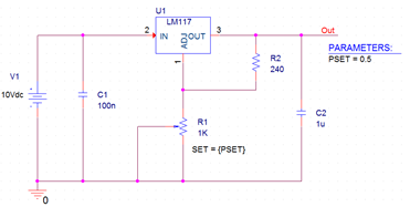
Figure 1: Linear potentiometer test circuit
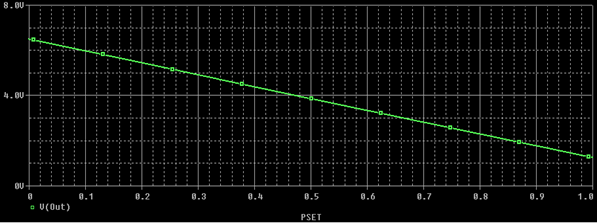
Figure 2: Simulation result for Linear potentiometer circuit
For this analysis, a DC sweep of the parameter PSET is used and PSET is swept from 0 to 1 in increments of 0.2.
So far we have assumed that the pot is linear, but for a logarithmic pot we need an extra parameter, that is, the dynamic range of the pot. The potentiometer can then be implemented by the following subcircuit.
.SUBCKT POT (TOP, BOTTOM, TAP) PARAMS: R=1K RANGE=1000 SET=.5
RTOP TOP TAP {R-(R/RANGE)*PWR(RANGE,SET)}
RBOT TAP BOTTOM { (R/RANGE)*PWR(RANGE,SET)}
.ENDS
As SET goes from 0 to 1, the value of RBOT goes logarithmically from R÷RANGE to R. RTOP makes up the difference between RBOT and the total resistance of the pot.
If a time-varying potentiometer is needed, it can be built using the same ideas as above. The subcircuit for time-varying potentiometer implements a voltage controlled resistance. One then builds an appropriate controlling waveform (using, for instance, the piecewise linear (PWL) type) to vary the resistance as desired.
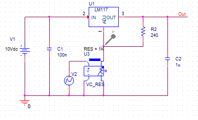
Figure 3: Time-varying potentiometer test circuit
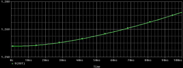
Figure 4: Simulation result for Time-varying potentiometer circuit
The simulation results show the change in resistance as a function of time versus the output voltage to be measured.
Variable resistors can also be used to implement many kinds of sensors. For example, a strain gauge, which consists of a resistance bridge, can be implemented using the following subcircuit:
.SUBCKT GAUGE (IN+ IN- OUT+ OUT-) PARAMS: R=1K F=0 SENS=1e-3
RUL IN+ OUT+ {R*(1+F*SENS)} ; upper left
RUR IN+ OUT- {R*(1-F*SENS)} ; upper right
RLL IN- OUT+ {R*(1-F*SENS)} ; lower left
RLR IN- OUT- {R*(1+F*SENS)} ; lower right
.ENDS
R can be determined by the gauge’s current drain (I) at the bias voltage (V), that is, R = V/I. SENS sets the sensitivity of the gauge and F is the applied force.

Figure 5: Strain Gauge Bridge Circuit
For example, as strain gauge is part of a pressure sensor, the full-scale output is 50 mV with a bias voltage of 10 V and the full scale corresponds to a pressure of 500 psi. Within the normal operating range, the bridge output is 10V*(F*SENS). In this case, with the full-scale output 50 mV at F = 500, the SENS = 50mV/(10V*500) = 10e-6.
Figure 6: Simulation result for Strain Gauge Bridge circuit
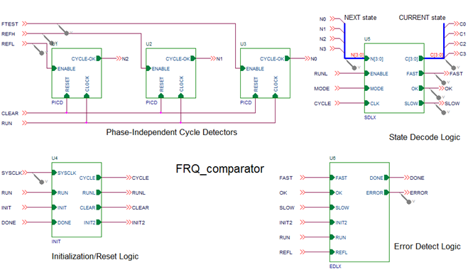
Figure 1: Top-level schematic for the frequency comparator circuit
The frequency-comparator circuit accepts two reference frequency inputs, and a test frequency input which is compared to the references. After initialization and start-up, the circuit produces fast, slow, OK, and error indications. Operation is continuous as long as both of the reference signals are applied. Initialization is accomplished by applying a low pulse to the INIT input, having a minimum width of 40 nsec. At least 40 nsec after the negative-going edge of the INIT input, circuit operation commences upon applying a negative-going edge to the RUN input. Outputs of the circuit–SLOW, FAST, OK, and ERROR–are pulses indicating the result of comparing the test frequency signal, FTEST, to the low and high frequency reference signals, REFL and REFH, respectively. The ERROR pulse is generated if more than 7 complete periods of the REFL signal are observed with no activity on the FTEST input during that time.
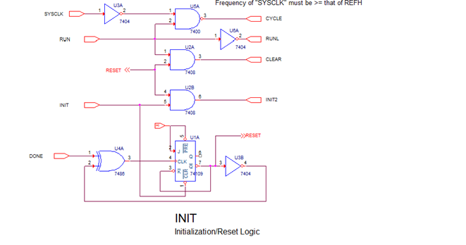
Figure 2: INIT block implementation
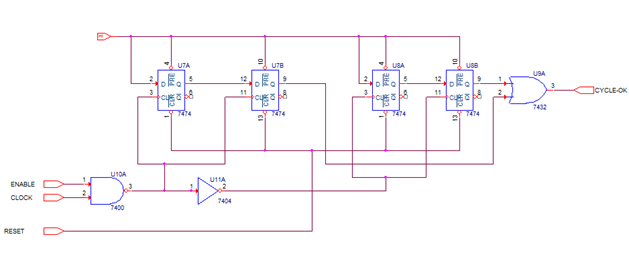
Figure 3: PICD block implementation
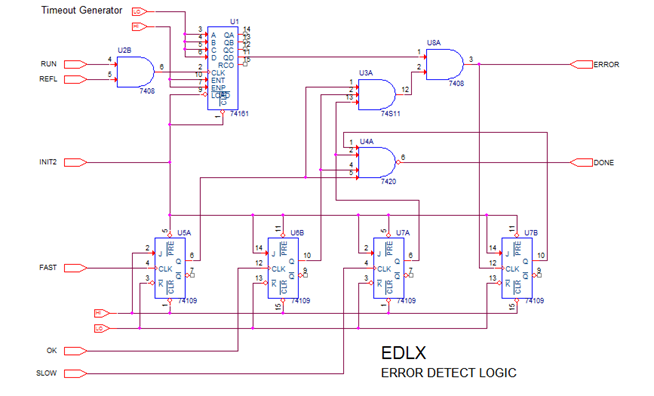
Figure 4: Error Detect Logic
The frequency-comparator circuit is designed in OrCAD Capture using hierarchical blocks for the initializer (INIT block), cycledetectors (PICD blocks), state-decoder (SDL block), and errordetector (EDL block). The design has two alternative implementations: a gate-level implementation using off-theshelf 74xx parts (see Figure 5), and a functionally equivalent implementation using a mixture of 74xx parts and a commonly available Programmable Array Logic (PAL) device, PAL20RP4B (see Figure 6). Both implementations use the digital stimulus include file,Freq_comparator.stm, providing definitions for the INIT, RUN, MODE, REFH, REFH, FTEST, and SYSCLK input signals. The design alternatives are implemented as two views of the SDL block, with the DEFAULT view being the gate-level implementation, and the PAL-IMPL view being the PAL implementation. For the PAL-IMPL view, the data required to program the PAL20RP4B device is supplied in a JEDEC file, FRQCHK.JED, generated using OrCAD/PLD.
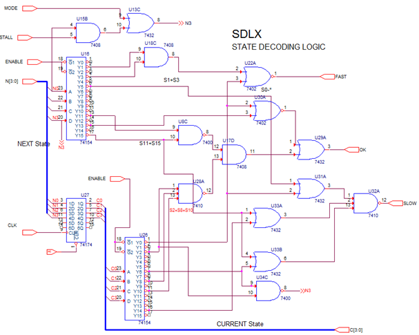
Figure 5: One implementation of the SDL block-the gatelevel view
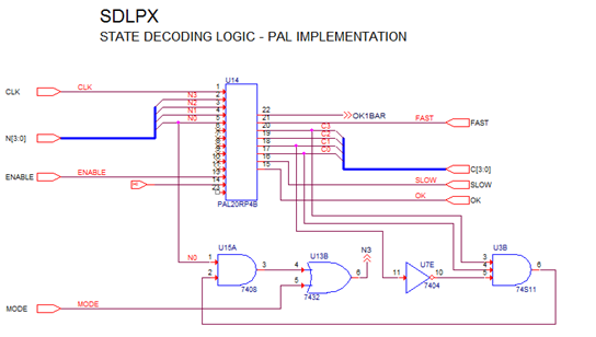
Figure 6: Another implementation of the SDL block-the PAL view
The three frequency inputs–REFL, REFH, FTEST–each drive a separate instance of a cycle-detector circuit (PICD blocks). Each cycle-detector is made up of two pairs of D-type flip-flops and a few basic gates. After having been reset and enabled, the cycle-detectors output a HI level as soon as two similar edges (e.g., falling) have been applied. This indicates that one complete period of the input signal has been observed. The circuit implements a simple finite-state machine (see Figure 7) that recognizes the order in which the individual frequency inputs make complete cycles.
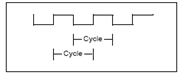
Figure 7: A Complete Cycle
For example, suppose that the REFH signal period is observed first (generating N1), followed by the REFL signal period (generating N2), then the FTEST period (generating N0). This indicates that the FTEST frequency is too low and that the SLOW output should be pulsed. But if the FTEST period is observed before the REFL cycle, an OK pulse is produced. The state machine current state simply represents the order of activity that has been observed since the last initialization or reset, which occurs every time any kind of output pulse is generated. The cycle-detectors monitor the input activity and produce the next state value (N3, N2, N1, N0), which is fed to the state-decoder (SDL block). At a rate determined by the system clock, SYSCLK, this next state becomes the current state; the 74154 4/16 decoders in the gate-level view of the state-decoder, continually provide unary logic indications of the next/current transitions (since next state values are not synchronized to SYSCLK). The random combinational logic in this same view recognizes the specific transitions that comprise the conditions of interest, i.e., FAST, SLOW, and OK, as per the state-transition diagram. (In the PAL view, the PAL20RP4B device replaces all of the decoding logic as well as the 4-bit register representing the current state value. The alternative implementations are functionally identical.) Note that the output indicators are not static state assignments; they are derived from selected state transitions. Thus, S14 þ S15 recognizes a SLOW condition, while S10 þ S15 signifies an OK condition.
The error-detector logic (EDL block) waits for the TIMEOUT signal output by the timeout generator. The timeout generator is simply a counter whose Q3 output indicates that the 8th rising edge of the low frequency reference, REFL, has occurred. If none of the normal output indicators (SLOW, FAST, or OK) have occurred before TIMEOUT, the ERROR output is asserted. The error-detector also asserts its DONE output whenever any of FAST, SLOW, OK, or ERROR have occurred.
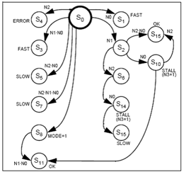
Figure 8: State transitions during frequency-comparator operations
The initialization/reset logic (INIT block) performs two functions. One distributes the effects of the INIT and RUN inputs, as defined in the stimulus include file, Freq_comparator.stm. The other uses the DONE signal from the error-detector to generate a RESET pulse; this has the same effect as the external RUN pulse–to restore the state machine to its starting state (0) as well as reset the cycle-detectors, timeout generator, and flip-flops in the error-detector. Normal operation then resumes.
JEDEC file containing the programming for the PAL20RP4B
OrCAD PLD 386
Type: PAL20RP4B
*
QP24* QF2568* QV1024*
F0*
L0000 11 11 11 11 11 11 11 11 11 11 11 11 11 11 11 11 11 11 11 01 *
L0040 11 11 11 11 11 11 11 01 11 11 11 01 11 11 11 11 11 11 11 11 *
L0080 11 11 11 11 11 11 11 11 11 10 11 11 11 11 11 11 11 11 11 11 *
L0120 11 11 11 11 11 11 11 11 11 11 11 11 11 10 11 11 11 11 11 11 *
L0320 11 11 11 11 11 11 11 11 11 11 11 11 11 11 11 11 11 11 11 01 *
L0360 10 11 10 11 11 11 01 01 11 01 11 01 11 01 11 11 11 11 11 11 *
L0640 10 11 11 11 11 11 11 11 11 11 11 11 11 11 11 11 11 11 11 11 *
L0960 11 11 10 11 11 11 11 11 11 11 11 11 11 11 11 11 11 11 11 11 *
L1280 11 11 11 11 10 11 11 11 11 11 11 11 11 11 11 11 11 11 11 11 *
L1600 11 11 11 11 11 11 10 11 11 11 11 11 11 11 11 11 11 11 11 11 *
L1920 11 11 11 11 11 11 11 11 11 11 11 11 11 11 11 11 11 11 11 01 *
L1960 10 11 01 11 10 11 01 01 11 01 11 01 11 01 11 11 11 11 11 11 *
L2000 01 11 01 11 01 11 01 10 11 10 11 10 11 11 11 11 11 11 11 11 *
L2240 11 11 11 11 11 11 11 11 11 11 11 11 11 11 11 11 11 11 11 01 *
L2280 01 11 01 11 10 11 01 01 11 01 11 01 11 01 11 11 11 11 11 11 *
L2320 01 11 11 10 01 11 01 11 11 11 11 11 11 11 11 11 11 11 11 11 *
L2560 11 11 11 11 *
C4B0E*
CCF0
Stimuli for the INIT, RUN, MODE, REFL, REFH, FTEST, and SYSCLK inputs
* "frqchk.stm" stimulus file
*
uh1 stim (4,1111) $g_dpwr $g_dgnd
+ INIT RUN MODE REFL
+ IO_STM IO_LEVEL=0
+ 0s 1100
+ 2055ns 0100
+ 2135ns 1000
+ 2175ns 1000
+ 2215ns 1000
+ 2255ns 1100
+ 5us 1101
+ label=loop1
+ +10us 1100
+ +10us 1101
+ +10us goto loop1 -1 times
uh2 stim (1,1) $g_dpwr $g_dgnd
+ REFH
+ IO_STM IO_LEVEL=0
+ 0s 0
+ +3us 1
+ label=loop1
+ +5us 0
+ +5us 1
+ +5us goto loop1 -1 times
uh3 stim (1,1) $g_dpwr $g_dgnd
+ FTEST
+ IO_STM IO_LEVEL=0
+ 0s 0
+ label=loop1
+ +20us 1
+ +20us 0
+ +20us goto loop1 5 times
+ +0s 1
+ label=loop2
+ +3us 0
+ +3us 1
+ +3us goto loop2 20 times
+ +0s 1
+ label=loop3
+ +6us 0
+ +6us 1
+ +6us goto loop3 10 times
uh5 stim (1,1) $g_dpwr $g_dgnd
+ SYSCLK
+ IO_STM IO_LEVEL=0
+ 0s 0
+ +2us 0
+ label=loop1
+ +800ns 1
+ +800ns 0
+ +800ns goto loop1 -1 times
The transient analysis is defined with: Print Step = 1us and Final Time = 1ms. All flip-flops must be initialized in the 0 state (rather than the default X state). This allows the simulator to properly initialize the circuit by forcing the reset logic to a deterministic state (non X; the hardware implementation would eventually syncronize itself to the input stimuli and operate correctly). In the top-level schematic, the SDL block is the only block with more than one view. Without further setup, OrCAD Capture will generate the PSpice netlist using the DEFAULT gate-level view for SDL. After running the simulation by PSpice, the state-machine operation is viewed in Probe by placing markers on the appropriate wires and buses, or by typing the signal names in the Probe dialog under the Trace/Add command as follows:
SYSCLK, REFH, REFL, FTEST
FAST, SLOW, OK, ERROR
{N3, N2, N1, N0} ;NEXT
{C3, C2, C1, C0} ;CURRENT
Figure 9 demonstrates the correct response of the circuit to the digital stimulus at FTEST.
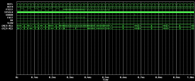
Figure 9: Frequency-comparator output FTEST input is Varied
© Copyright 2015 Cadence Design Systems, Inc. All rights reserved. Cadence, the Cadence logo, and Spectre are registered trademarks of Cadence Design Systems, Inc. All others are properties of their respective holders.
1766 12/13 CY/DM/PDF
Copyright © 2024 Cadence Design Systems, Inc. All rights reserved.