Here you will find out latest app notes.
In high-speed signal transmission, understanding transmission line behavior is imperative to achieving proper impedance matching and proper termination to minimize loss stemming from reflections, as well as to maximize signal integrity. This paper shows that transmission line behavior can be accurately modeled using simple SPICE simulations with an inductance (L) and capacitance (C) network, and also provides a good physical understanding of the mechanism of reflections and derivation of key formulas.
A transmission line can be broken down into a network of distributed L, C, and resistance (R) elements. It’s important to achieve an intuitive and physical understanding of how and why a transmission line behaves as it does, to demystify the reasons for its characteristics, and to gain an in-depth understanding in terms of its fundamental elements. In other words, L and C (for a lossless transmission line) is very important.
In order to gain a deeper understanding of the way that a transmission line functions and what makes it unique compared to a normal conductor, I performed some SPICE simulations, where I plugged in simple LC networks to model a transmission line. I experimented with different kinds of stimuli and observed the propagation of signals at each point on the transmission line. In this paper, I describe the experiments I’ve done and the deeper insights I’ve gained as a result of accurately modeling full transmission line behavior using a simple LC network. All of the expressions, such as the reflection coefficient, can be derived fully using fundamental properties of capacitors and inductors, as well as energy conservation principles. Such work provides a physical idea as to how the mechanism of reflections in the transmission line occur.
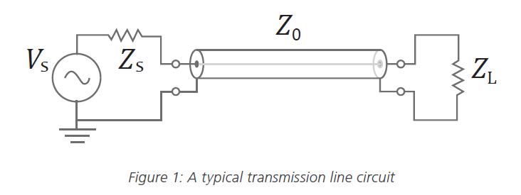
In addition to modeling the transmission line as a simple passive LC network, I also used PSpice® technology from Cadence to perform simulations (See Figure 1 for a depiction of a typical transmission line circuit). I attempted to analyze both the forward and reflected traversals of the signal input. To understand the derivation of expression for the reflection coefficient for reflection at the load, I tapped into the principle of energy conservation.
For this work, I examined the following cases:
A good derivation for the characteristic impedance of a transmission line is available here. From the derivation, for a forward propagating wave, we see that V(x)/I(x) is not a function of t, nor even of x. For a lossless transmission line, at any x, V/I = √(L/C). As far as the source of V(0,t) is concerned, the transmission line behaves in exactly the same way as a resistor of value √(L/C). We call this resistance the characteristic impedance of the transmission line.
L and C are the distributed inductance/unit length and capacitance/unit length of the transmission line, respectively. A handy rule of thumb to determine if an interconnect trace should be considered a transmission line is if the interconnect delay is greater than 1/8th of the signal transition time; in this case, it should be afforded all of the attention required by a transmission line.
If the propagation delay time is much smaller, the voltage gradient across the interconnect between the two ends of the interconnect for a given input signal will be much smaller. As a result, a lumped approach can be taken, and the interconnect need not be taken as a transmission line.
For this work, I assumed a lossless transmission line. For the simulations, I used a network of 320 cascaded LC sections. A section of it is illustrated below in Figure 2.

The value of a single inductance element=0.05nH and that of a single capacitor element=0.02pF, such that the characteristic impedance Z0= √(L/C)=50ohms. The total one-way delay=n* √(LC)=320ps here (n=number of LC segments). A source resistance Rs=200 is used here to illustrate the case of reflections at the source side.
Please note that the values of the single inductance and capacitance elements for an ideal transmission line will be much smaller than the values used here; these values are used here for ease of simulation and for us to be able to better observe the results.
Let’s apply an input step of 0-1V by the voltage source at time t=100ps. The rise time assumed is 1fs for this step. As we saw before, for the step incident at the transmission line input, the transmission line behaves in exactly the same way as a resistor of value √(L/C)=Z0=50ohms. So, as far the source is concerned, the equivalent circuit right at the instant of application of the step is as depicted in Figure 3.
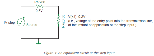
So the 1V step is split as 0.8V across Rs and 0.2V across R=Z0 right at the entry point into the transmission line, by simple resistive voltage division action.
Now, let us examine the process of propagation of this step injected into the transmission line. As far as the advancing voltage step is concerned, on the transmission line, at any instant of its propagation to the other end until it reaches the end, the impedance=Z0=50 ohms.
Right at the entry point of the transmission line, the input current is a constant current=V/(Rs+Z0). Now, as far as the very first two LC segments in the transmission line are considered, the equivalent circuit as depicted in Figure 4.

In other words, it is equivalent to a constant current source=V/(Rs+Z0) driving a parallel RC combination, where R=Z0 and C=the first unit capacitance.
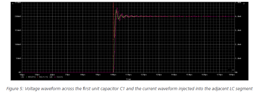
Now the voltage across the first unit capacitor increases exponentially with a time constant=RC=Z0C, and the current taken by this capacitor decays exponentially to zero. At the same time, the current injected into the adjacent LC segment increases exponentially. The sum of the two currents is still V=(Rs+Z0).
The voltage waveform across the first unit capacitor C1 and the current waveform injected into the adjacent LC segment observed from simulation is illustrated below in Figure 5. The purple waveform is the voltage across the first unit capacitor C1, the green waveform is the current injected into the second LC segment, and the red waveform is the voltage step input applied at t=100ps, probed right at the input of the transmission line (0.2V):
As seen earlier, the input current into the second LC segment is an exponential one with time constant=Z0C. Now the equivalent circuit for the second and third LC segments becomes:

The current into the second unit capacitor C2 initially increases with an increasing exponential profile to a point, after which the current shunted away from it by R=Z0 starts becoming significant and the current into C2 starts reducing and finally becomes 0, at which point voltage across C2=V*Z0/(Rs+Z0) =0.2V in this case.
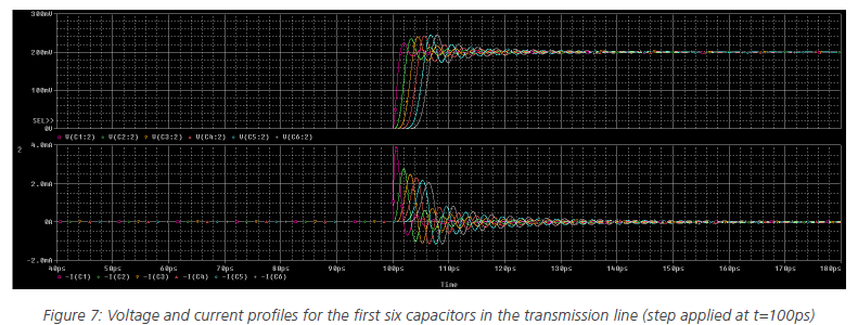
The voltage and current profiles for the first six capacitors in the transmission line are illustrated below in Figure 7. The screen shot shows that the rise time of the voltage waveform keeps on slowing down as we progress down the transmission line, due to the change in profile of the currents going into each capacitor as we move down the transmission line. In this manner, the step input injected into the transmission line propagates towards the end. Note that during this process, the nature of termination of the transmission line is immaterial until the propagating wave reaches at the end of the transmission line. Until that point, during its traversal, the propagating waveform is blind to the kind of termination on the transmission line and can only see Z0 at each point it reaches.
As mentioned before, for a step input injected into the transmission line, the nature of termination of the transmission line is immaterial until the propagating wave reaches at the end of the transmission line. Until that point, during its traversal, the propagating waveform is blind to the kind of termination on the transmission line and can only see Z0 at each point it reaches. As far as the starting point x=0 of the transmission line is concerned, until a round trip delay time = 2Td=2n√(LC), the impedance seen by the voltage source at x=0 is Z0 itself, irrespective of the type of termination. Hence, a constant current=V/(Rs+Z0) is continuously injected into the transmission line entry point all during this time (Td=transmission line delay, n is the number of LC segments, and L and C are the unit inductance and capacitance values per segment). The voltage at this point x=0, i.e., right at the entry point of the transmission line, it remains V*Z0/(Rs+Z0) during this time, irrespective of the kind of termination of the transmission line.
Starting right from the step input application instant, for a time duration= the round trip transmission line delay time = 2Td=2n√(LC), the energy injected by the voltage source into the transmission line is V*I*t=V1I12n√(LC), where V1,I1 are the voltage and current, respectively, at point x=0. That is, the entry point of the transmission line, n, is the number of LC segments, and L and C are the unit inductance and capacitance values per segment.
By the principle of energy conservation, this is the total available energy to be stored in the inductors and capacitors within the transmission line and to be dissipated in the final load resistance RL, with which the transmission line is terminated during this time duration. This is illustrated in Figure 8.

When the step input finally reaches the end of the transmission line, depending on the value of the termination resistance RL, the voltage at the end point becomes V2. Now the current drawn by the load resistance settles at I2=V2/RL. Starting from the
nearest LC segment to the output load, the current in the inductors and the voltage across the capacitors start settling to I2 and V2, respectively, and this keeps on happening on all the inductors and capacitors gradually moving towards the source. Actually, this is, in fact, the mechanism of reflection. I will discuss reflections more later on.
After a round dip delay time of around 2Td=2n√(LC), the currents in all the inductors and voltage across all the capacitors should have settled to I2 and V2, respectively. Now, the total energy stored at the end of 2Td in the LC network is given 
where n is the number of LC segments and L and C are the unit inductance and capacitance per segment, analogous to the inductance/unit length and capacitance/unit length. But I2=V2/RL, thus the total energy stored at the end of 2Td in the LC network is given by  .
.
Regarding the energy dissipated in the load resistance RL during 2Td, note that current starts flowing across RL only after the first Td has been completed, i.e. it is=0 for the first Td, and it only flows during a time period of Td after that. Thus, the energy dissipated in RL during this time period is given by:

Now, using the principle of energy conservation as mentioned in the previous slide, the energy injected by the voltage source into the transmission line during 2Td is V*I*t=V1*I1*2n√(LC)= The total available energy stored in the inductors and capacitors within the transmission line during 2Td + total energy dissipated in the final load resistance RL during 2Td, i.e.:
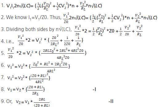
This is the expression for the voltage at the output of the transmission line V2 after the first delay Td, i.e., after the transmitted step input first reaches the output load. Reflection coefficient is given by the ratio of the amplitude of the reflected wave (V2-V1) to the incident wave (V1), i.e. reflection coefficient ρ= (V2-V1) / V1. Setting

We saw previously that when a step input is first injected into the transmission line, once it reaches the output end, the voltage at the output end reaches a value V2 depending on the value of the load termination resistance, whose expression was derived using the principle of energy conservation. Now, starting from the nearest LC segment to the output load, the current in the inductors and the voltage across the capacitors start settling to I2=V2/RL and V2, respectively, and this keeps on happening on all the inductors and capacitors gradually moving towards the source.
Actually, this is in fact the mechanism of reflection, and in this manner the new voltage V2 propagates towards the source end gradually, LC segment by LC segment. Thus, the voltage step which started out as V1 at the transmission line input gets modified to V2 upon reaching the end of the transmission line. The reflected step injected back into the transmission line from the load end has an amplitude of V2 - V1, and this step propagates towards the source end. The step on reaching the source end modifies the voltage at the source end, i.e. at the input of the transmission line from the source side, to a new voltage V3 due to reflection at the source end depending on the source resistance.
To find the expression for this new voltage V3 at the input of the transmission line after the first reflection at the source end, we can again make use of the principle of energy conservation and also the principle of superposition. There is already a voltage V1 right from the instant of application of the initial step input from the source at the input of the transmission line. This has to be superimposed with the voltage step at the source side due to source reflection, to find the net new voltage V3 at the input of the transmission line, i.e. at x=0. To find the step voltage change alone at the source end due to the effect of reflection at the source, let us first short out the main source. The effective circuit is illustrated in Figure 9. The amplitude of the step injected back into the transmission line due to reflection at the load is V2-V1=V2’:

Starting right from the reflected step input application instant from the load side, for a time duration = the round trip transmission line delay time = 2Td=2n√(LC), the energy injected by the reflected step into the transmission line is V*I*t=V2’I2’2n√(LC), where V2’,I2’ is V2-V1 and (V2-V1)/Z0, respectively. In other words, the amplitude of the voltage step injected back by reflection at the load end, and the effective current injected back due to this reflected step (this current is actually the delta between the current drawn by the output load and the current initially drawn by the transmission line from the main source = V/(Z0+Rs), due to the effect of load reflection), n is the number of LC segments, and L and C are the unit inductance and capacitance values per segment.
By the principle of energy conservation, this is the total available energy to be stored in the inductors and capacitors within the transmission line and to be dissipated in the source resistance Rs with which the transmission line is terminated. In this consideration, we are neglecting the energy stored within the LC network due to the main step from the source side. We are only considering the energy freshly injected into the LC network by the reflected load step, for applying the principle of superposition. Let the new voltage at the source end of the transmission line (due to the reflected load step alone, ignoring the effect of the main source by shorting it out) be V3’.
Following the same approach we used before:
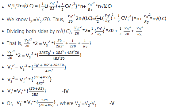
This is the expression for new voltage at the source end of the transmission line (due to the reflected load step alone, ignoring the effect of the main source by shorting it out) after the first delay Td, i.e. after the load reflected step first reaches the source end. Superimposing the effect of the actual source, too, the actual voltage at the source end after the first source reflection is given by V3=V3’+V1, where V1 is VZ0/(Z0+Rs) (V being the amplitude of the original step from the main source). The reflection coefficient at the source side is given by the ratio of the amplitude of the reflected wave from the source end (V3-V2) to the incident wave (V2-V1), i.e. reflection coefficient at the source end ρ= (V3-V2) / (V2-V1).


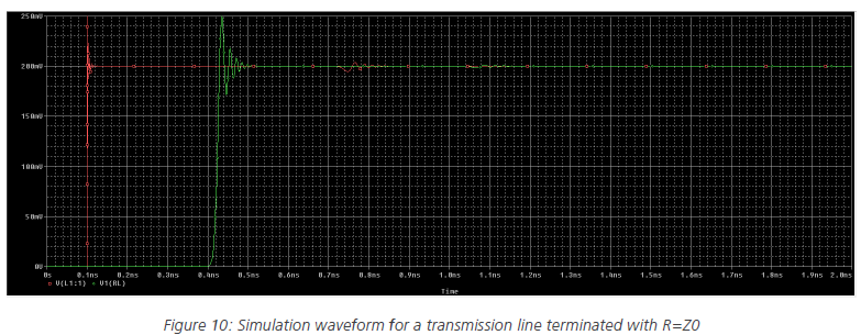
The source resistance is 200ohms. As seen in the simulation waveform below (Figure 10), the final output across the 50ohm load R=Z0 (the green waveform) directly goes to the final voltage=0.2V after about 320ps from the input step edge at t=100ps (the red waveform). No reflection is observed.
NOTE: In an actual transmission line, the rise time of Vout will be much smaller than as seen in the waveform in Figure 10, and will almost look like a vertical edge, because the unit inductance and capacitance values are much smaller than the ones used in the LC model here.
Also, some amount of ringing is noted here both at the transmission line input point and at the load, due to the ultra fast rise time of the step inserted and the non-infinitesimally small values of L, C we have used in this simulation.
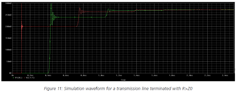
The source resistance is 200ohms. Here, the output of the transmission line is terminated with R>Z0=75 ohms. As seen in the simulation waveform below in Figure 11, the final output across the 75ohm load (the green waveform) as well as the voltage right at the input of the transmission line (the red waveform) arrives at a final settled voltage of around 272.73mV after a series of reflections.
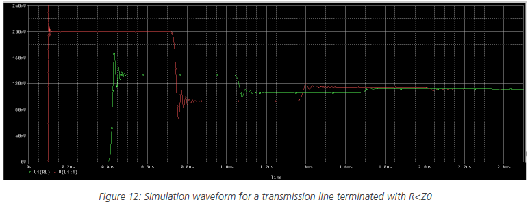
The source resistance is 200ohms. Here, the output of the transmission line is terminated with R<Z0=25 ohms. As seen in the simulation waveform below in Figure 12, the final output across the 25ohm load (the green waveform) as well as the voltage right at the input of the transmission line (the red waveform) arrives at a final settled voltage of around 111.11mV after a series of reflections.
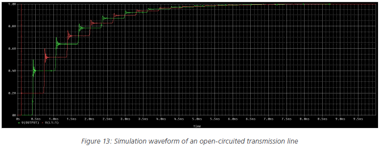
The source resistance is 200ohms. Here, the output of the transmission line is open circuited. As seen in the simulation waveform below in Figure 13, the final output at the transmission line output node (the green waveform) as well as the voltage right at the input of the transmission line (the red waveform) arrives at a final settled voltage of 1V after a series of reflections.
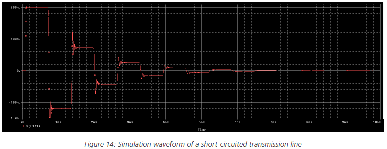
The source resistance is 200ohms. Here, the output of the transmission line is short-circuited. As seen in the simulation waveform below in Figure 14, the voltage right at the input of the transmission line (the red waveform) arrives at a final settled voltage of 0V after a series of reflections.
The source resistance is 200ohms. Here, the output of the transmission line is terminated in a capacitor of value C. This is a special scenario. When the transmission line is terminated in a resistance=R, the injected step input on reaching the end of the transmission line is met by a constant impedance=resistance R at that instant. But in the case of a capacitance termination, the capacitor provides a time-varying impedance to the injected step input arriving at the transmission line end. This is explained below.
Right at the instant the step reaches the capacitor, the impedance provided by the capacitor is zero because the capacitor acts as a short at that instant, preventing any instantaneous change of voltage across it. So, right at the instant the step reaches the capacitor, the system is analogous to a transmission line whose output is short-circuited. Now as the capacitor starts charging, the impedance provided by the capacitor, i.e., the ratio of the current into the capacitor to the voltage, keeps on changing, as per the variation in the current into the capacitor and the voltage across it. It is possible to derive the equation governing the voltage across the load capacitor, which gives the nature of variation of this voltage with respect to time. This is a particularly important result. This derivation is shown later on. Please note that this equation holds true from t=T0+Td, (where T0 is the instant of application of the original step input) to t=T0+3Td. This is because the capacitor starts charging from the instant where the original step reaches the end of the transmission line, i.e., t=T0+Td, and it can charge exactly as per this equation for a duration=round-trip delay time 2Td, after which the waveform gets disturbed by the reflected wave from the source end in response to the wave initially reflected from the load end.
Let’s revisit equation num “II,” which was presented earlier:  This is the expression for the voltage at the output of the transmission line V2 after the first delay Td, i.e., after the transmitted step input first reaches the output load. V1 is the amplitude of the step initially injected into the transmission line, given by V*Z0/(Z0+RS), where V is the amplitude of the step from the main source. From the instant the originally injected step reaches the load end, to the instant when the reflected step from the source end in response to the reflection from the load end reaches back at the load end, the duration is 2Td. At any time during this time interval, if the value of the load resistance RL changes, V2 will change accordingly as per
  .
.
Let’s replace RL in the equation by a generic load impedance ZL, where ZL is given by V2/I2, i.e. the ratio of the voltage across the load to the current going into the load. In this derivation, we are going to make use of the idea that the capacitor presents itself as a time-variable impedance, which is dependent on the voltage across it. So, we have to consider the instantaneous impedance ZL(t).
1. Let V2(t) be the voltage across the capacitor at time t. Now, 
2. For a capacitor, the current through it I=CdV/dt, where V is the voltage across it. Thus, the impedance of the capacitor=V/I=V/(CdV/dt). Applying this principle for ZL(t), ZL(t)=V2(t)/(CdV2(t)/dt), where C is the value of the load capacitor, and V2(t) the instantaneous voltage across the capacitor at time t.
3. Substituting for ZL, 
4. Z0+ V2(t)/(CdV2(t)/dt)=2V1/(CdV2(t)/dt)
5. Z0CdV2(t)/dt+V2(t)=2V1
6. Taking Laplace transform on both sides, we get V2(s) + sZ0CV2(s)=2V1(s)/s. Please note it is assumed initial voltage at time t=0 across the capacitor C is 0V here.
7. i.e., V2(s)(1+sZ0C)=2V1(s)/s
8. So V2(s) = 2V1(s)/(s(1+sZ0C)) = 2V1(s)/(sZ0C(s+1/Z0C))
9. Making use of partial fractions, 2V1(s)/(sZ0C(s+1/Z0C)) = A/sZ0C + B/(s+1/Z0C)
10. Thus, A(s+1/Z0C) + BsZ0C =2V1(s)
11. Letting s=0 and s=-1/Z0C, we get A=2V1(s)Z0C and B=-2V1(s)
12. Substituting for A and B in the equation for V2(s) , V2(s) =2V1(s)Z0C/sZ0C - 2V1(s)/(s+1/Z0C)
13. i.e., V2(s) =2V1(s)/s - 2V1(s)/(s+1/Z0C)
14. Taking inverse Laplace transform, V2(t) = 2V1(t) - 2V1(t)(e-t/Z0C) = 2V1 - 2V1(e-t/Z0C) , because V1 is a constant.
15. Thus, finally we get: V2(t) = 2V1(1-e-t/Z0C)
This is the equation governing the voltage across the load capacitor, which gives the nature of variation of this voltage with respect to time. As noted before, this equation holds true from t=T0+Td, (where T0 is the instant of application of the original step input) to t=T0+3Td. This is because the capacitor starts charging from the instant where the original step reaches the end of the transmission line, i.e. t=T0+Td, and it can charge exactly as per this equation for a duration=round-trip delay time 2Td, after which the waveform gets disturbed by the reflected wave from the source end in response to the wave initially reflected from the load end. Thus, it is clear that capacitor charging follows a typical simple RC-type exponential charging, with the time constant being Z0C. We know that for such a charging profile, the voltage across a capacitor varies as per Vfinal(1-e-t/RC), and the current into it varies as per Iinitial(e-t/RC). Now, taking the ratio, the impedance provided by the capacitor follows a profile given by k(et/ RC-1), where k is a constant=Vfinal/Iinitial. The simulated waveform for this impedance variation profile is given for a load cap of 2pF below in Figure 15:
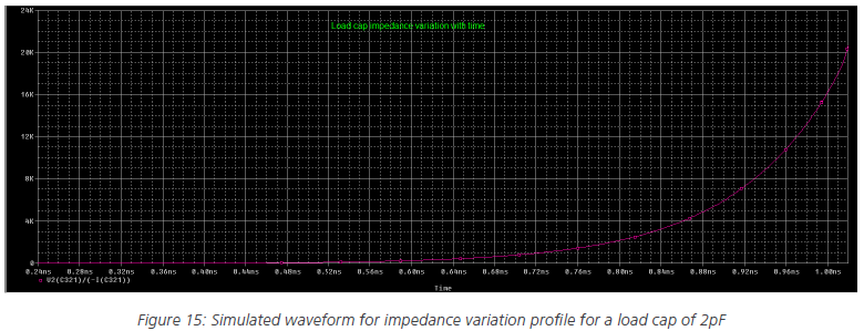
Even this impedance sees an exponential time-variation profile, with a time constant=Z0C itself. Thus, at the output of the transmission line, the voltage exponentially charges from 0V (what the output voltage of the transmission line would’ve been for a shortened transmission line) to whatever voltage the output end would have gone to were the transmission line output open-circuited, with a time constant=Z0C.
We can now predict the nature of the voltage variation at the output. Now, making use of the knowledge that the capacitor provides an exponentially varying impedance at the output with a time constant Z0C, we can also predict how the voltage at the source end of the transmission line changes once the reflected waveform from the load reaches it. Since the impedance provided by the capacitor starts off at 0 ohms, at first, as the reflected wave reaches back to the source end, the voltage at the source end would go to whatever voltage it would have gone to upon receiving the first reflection from the load side, for a short-circuited transmission line.
As the capacitive impedance increases exponentially with a time constant Z0C, the voltage at the source end would go to whatever voltage it would have gone to upon receiving the first reflection from the load side, for a transmission line terminated in a resistance R=the instantaneous impedance of the capacitor at that time. Thus, the voltage at the source end also follows an exponential RC charging profile with time constant=Z0C. Finally, since the impedance provided by the capacitor is infinity, i.e. open circuit, once it has charged to its final voltage, the voltage at the source end would go to whatever voltage it would have gone to upon receiving the first reflection from the load side, for an open-circuited transmission line. In this manner, source and load reflections continue until the output settles to the final value.
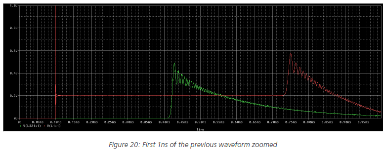
The simulation waveforms for the load end voltage (green waveform) and source end voltage (red waveform), for a 1V step injected into a 50ohm Z0 transmission line with delay=300ps, is given in Figure 16. A zoomed version of the initial portion of these waveforms is presented in Figure 17. Source resistance used is 200ohms, and output capacitor is 1pF.
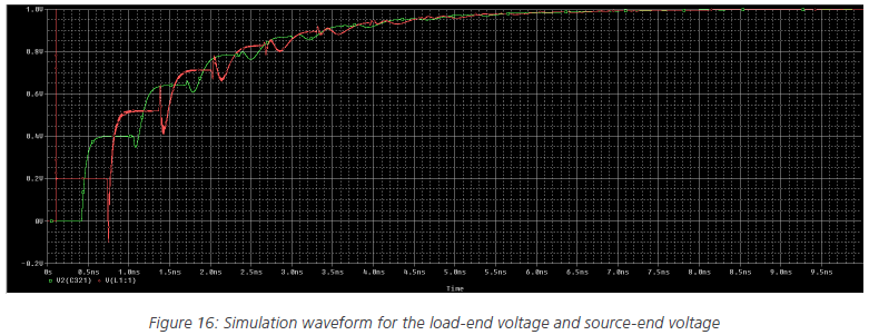
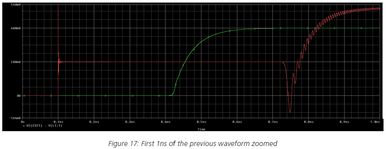
One important thing we have to consider here is the transmission line delay Td. It is to be noted that the output capacitor starts charging only after a time period= Td after the instant of injection of the original step input into the transmission line. The total time available for the output capacitor to charge freely as per Z0C until the charging process gets disturbed by the reflected wave from the source end is equal to the time taken for the initial reflected wave from the load to reach the source and get reflected back to the load from the source, which equals a round dip delay time of 2*Td.
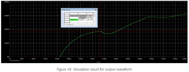
Making use of this knowledge, we can easily predict the final voltage the output capacitor reaches before it gets disturbed by the reflected wave from the source end, for any given transmission line delay Td. We can use the basic capacitor RC charging equation, Vfinal(1-e-2Td/Z0C), where Vfinal is the voltage the output end of the transmission line would have reached for an open-circuited transmission line. This idea can be further extended to predict the profiles for each step in the reflected waveform both at the transmission line input as well as output. To illustrate an example, let’s consider a 1V step injected into a 50ohm Z0 transmission line with delay Td=70ps, with source resistance =200ohms and output capacitor 1pF. Here Vfinal expected is 0.4V just after step reaches the output end, for an open-circuited transmission line. Thus, we can predict that the final voltage the output capacitor reaches before it gets disturbed by the reflected wave from the source end is Vfinal(1-e-2Td/Z0C)= 0.4 (1-e-2*70ps/50*1pF) =~375.6mV. (This is observed to match the simulation result for the output waveform for this case, as observed in the waveform in Figure 18.)
The initial portion of the simulation waveforms for the load end voltage (green waveform), for a 1V step injected into a 50ohm Z0 transmission line with delay=70ps, with source resistance =200ohms and output capacitor 1pF, showing the capacitor voltage charging to Vfinal(1-e-2Td/Z0C)= 0.4 (1-e-2*70ps/50*1pF) =~0.376V, before it gets disturbed by the reflection from the source side.
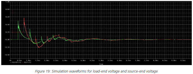
An approach similar to the capacitor termination case can be taken for a transmission line terminated in an inductor L, too. Only here, the time constant is L/Z0 and the impedance initially starts off as an open circuit, and decays exponentially to zero, finally following a time constant of L/Z0.
As shown in Figure 19, the simulation waveforms for the load-end voltage (green waveform) and source-end voltage (red waveform), for a 1V step injected into a 50ohm Z0 transmission line with delay=300ps, with source resistance =200 ohms and output inductor, is 10nH.
As demonstrated in this paper, transmission line behavior can be accurately modeled using simple SPICE simulations in an LC network. A better understanding of transmission line behavior is important for achieving proper impedance matching and proper termination to minimize loss from reflections and also to maximize signal integrity. In addition, a deeper understanding of transmission lines will enable you to better understand and interpret results from signal integrity tools, such as those in the Cadence® Sigrity™ product line.
Simulation tools used: PSpice technology from Cadence
© 2016 Cadence Design Systems, Inc. All rights reserved worldwide. Cadence, the Cadence logo, and PSpice are registered trademarks and Sigrity is a trademark of Cadence Design Systems, Inc. All others are properties of their respective holders. 6555 04/16 CY/DM/PDF
Copyright © 2024 Cadence Design Systems, Inc. All rights reserved.
