Here you will find out latest app notes.
The length of time it takes to perform a transient simulation on a high-Q oscillator circuit makes simulation inefficient. The dominant time constant of the circuit, due to the Q of the crystal, means that the simulation must run a minimum of Q cycles before the circuit reacts. And, because you must wait Q cycles, there is no way to force an oscillator to a steady state condition. For a crystal with moderately high-Q (20,000), it can take close to a million cycles before the oscillator reaches a steady state condition. Besides the long time required for the simulation to run, the data file created by the simulation will be extremely large. But, it is possible to use AC analysis to simulate high-Q circuits. These results can be used to investigate whether the loop gain and phase are conducive to producing a stable oscillation.
The circuit can be analyzed by injecting a current to measure the current gain, and a voltage to measure the voltage gain of the circuit. Previously, the circuit to be analyzed was treated as a subcircuit, with the signal path, broken to make measurements, pulled out. The subcircuit was then used twice: once so that a voltage could be injected, and again so that a current could be injected.
Note: This approach of measuring loop gain relies on the voltage and current feedback theory as described in detail in A Guide to Circuit Simulation and Analysis Using PSpice, references [1] and [2].
Another approach of measuring the loop gain is to create a subcircuit for the device that is used to make the measurements, then reinsert this subcircuit into the circuit to be analyzed. The loop gain subcircuit, consisting of two voltage sources and one current source, is as follows:
.SUBCKT LGT A B PARAMS: VOLTS=0
V1 1 A DC 0 AC {VOLTS}
V2 1 B DC 0 AC 0
I1 1 0 DC 0 AC {1-VOLTS}
.ENDS
When the value of the VOLTS parameter is equal to 0, the I1 current source will have a value of 1, and voltage sources V1 and V2 will have a value of 0. This condition allows measurement of the current gain of the circuit. Sources V1 and V2 will be used to sense the input current and the output current of the circuit. The current gain of the circuit is determined with the following equation:
Ti = I(V1)/I(V2)
When the value of the VOLTS parameter is equal to 1, the V1 voltage source will have a value of 1, and the I1 current source will have a value of 0. This condition allows measurement of the voltage gain of the circuit. The voltage gain is the ratio of the voltages measured at the nodes of the subcircuit.
Tv = V(A)/V(B)
Note: To perform the current gain and the voltage gain portions of the analysis, it is necessary to perform a parametric analysis in addition to the AC analysis. This can be accomplished by placing a PARAM symbol on the schematic. In the example circuit shown in Figure 2, the parameter is named ACVAL, and the default value is set to 0. The parametric sweep is set to run the AC analysis with the global parameter ACVAL set to each of the values defined in the value list. The value list for this analysis contains two values: 0 and 1.
Once the voltage gain and the current gain are calculated, the total loop gain can be determined by the following relation:
1/T+1 = 1/Ti+1 + 1/Tv+1
Therefore,
T=((Ti+1)||(Tv+1)) - 1
where
x||y = 1/(1/x + 1/y) = xy/(x+y)
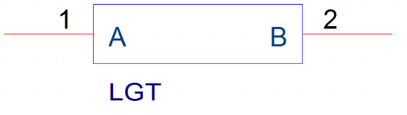
Figure 1: Symbol Graphic
The symbol contains the attribute VOLTS = 0. This parameter is used to pass the value of a global parameter to the subcircuit. In the example circuit, the global parameter ACVAL is defined and the attribute value of VOLTS is set to {ACVAL}. If a parameter value is not passed to the subcircuit, the default value for VOLTS is then 0. The template for the symbol is as follows (as a single line):
X^@REFDES %A %B @MODEL PARAMS: ?VOLTS|VOLTS=@VOLTS||VOLTS=0|
Figure 2 shows a 100 kHz crystal oscillator circuit with a Q of 20,000. To analyze this circuit, the LOOPGAIN subcircuit is inserted into the feedback path. The A node is connected to the output side of the feedback path and the B node is connected where the feedback is summed into the circuit. If the subcircuit is inserted backwards, the results will show a loss, or be upside down. The AC analysis is set up to sweep the circuit from 99.9 kHz to 100.1 kHz using a linear sweep of 100 points.
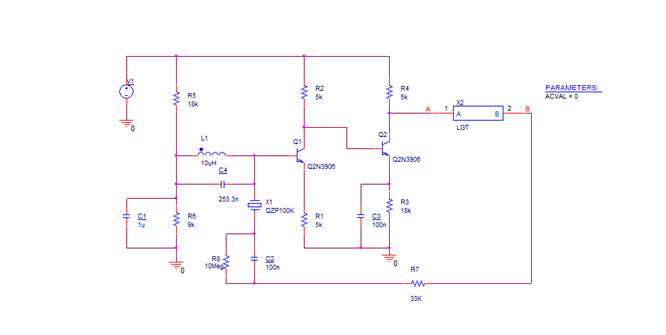
Figure 2: 100Khz crystak oscillator circuit
After the analysis is complete, the results may be viewed using Probe. The following Probe macros can be defined:
par(a,b)=(((a)*(b))/((a)+(b)))
Ti = ((I(X_X2.V1)@1)/I(X_X2.V2)@1)
Tv = (V(A)@2/V(B)@2)
T=(par(Ti+1,Tv+1)-1)
The macro par(a,b) defines the parallel combination of the arguments a and b.
The simulation results (Figure 3) for the oscillator circuit show the peak gain and a 180 degree phase shift at the resonant frequency of the crystal.
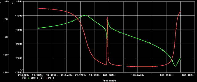
Figure 3: Example Circuit's Simulation Results
References
[1] Paul W. Tuinenga, SPICE: A Guide to Circuit Simulation and Analysis Using PSpice. Prentice-Hall, 1988, pages 59-65.
[2] Paul W. Tuinenga, SPICE: A Guide to Circuit Simulation and Analysis Using PSpice. Second Edition, Prentice-Hall, 1992, pages 81-88.
© Copyright 2016 Cadence Design Systems, Inc. All rights reserved. Cadence, the Cadence logo, and Spectre are registered trademarks of Cadence Design Systems, Inc. All others are properties of their respective holders.
Copyright © 2020 Cadence Design Systems, Inc. All rights reserved.